
onsemi
NB3V8312CMNG

Why Choose Us?
Professional Platform
B2B & B2C purchasingDelivery at full speed
1-2 days deliveryWide variety
Original manufacturers365 days guarantee
Responsible quality
.png)


Tech Specifications
NB3V8312CMNG Description
NB3V8312CMNG Description
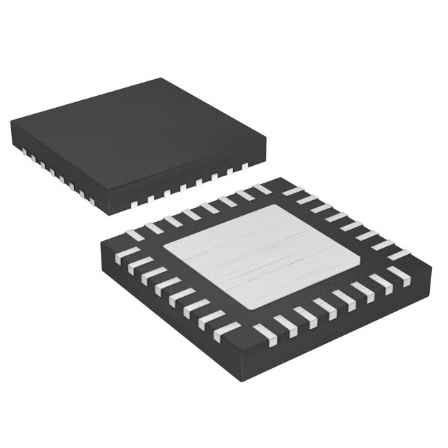
The NB3V8312CMNG from onsemi is a high-performance 1:12 fanout buffer designed for clock distribution in demanding electronic systems. This surface-mount IC operates within a 1.6V to 3.465V supply range, making it compatible with LVCMOS and LVTTL input signals while delivering LVCMOS outputs. With a maximum frequency of 250 MHz, it ensures precise signal integrity for high-speed applications. Packaged in a 32-QFN tube, the device is RoHS3 compliant and rated MSL 1 (Unlimited), ensuring reliability in manufacturing and assembly.
NB3V8312CMNG Features
- 1:12 Clock Distribution: Provides low-skew, high-fanout signal replication for synchronized system timing.
- Wide Voltage Range (1.6V–3.465V): Supports mixed-voltage designs, enhancing flexibility in FPGA, ASIC, and processor-based systems.
- LVCMOS/LVTTL Compatibility: Ensures seamless integration with common logic standards.
- 250 MHz Max Frequency: Ideal for high-speed data transmission and low-jitter clock networks.
- Surface-Mount 32-QFN Package: Compact footprint suitable for space-constrained PCB layouts.
- Robust Compliance: RoHS3, REACH Unaffected, and ECCN EAR99 certified for global deployment.
NB3V8312CMNG Applications
- Telecommunications: Clock tree distribution in 5G base stations and network switches.
- Data Centers: Synchronization of servers, storage systems, and high-speed interconnects.
- Consumer Electronics: Timing control in gaming consoles, smart TVs, and set-top boxes.
- Industrial Systems: Precision clocking for automation controllers and test equipment.
- Automotive Infotainment: Low-jitter clock distribution in ADAS and in-vehicle networks.
Conclusion of NB3V8312CMNG
The NB3V8312CMNG stands out as a high-reliability, low-power solution for clock distribution in advanced electronic systems. Its wide voltage range, high fanout capability, and robust compliance make it superior to competing models in jitter-sensitive and mixed-voltage environments. Whether for data-intensive, industrial, or consumer applications, this buffer ensures timing accuracy and system stability, solidifying its role as a critical component in modern digital designs.
FAQ
Not available to buy online? Want the lower wholesale price? Please Send RFQ to get best price, we will respond immediately


.png?x-oss-process=image/format,webp/resize,h_32)


