
 German
 Japanese
 Portuguese
 Korea
Korea
 Mexico
 Dutch
Dutch


onsemi
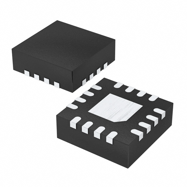
NB7L11MMNR2G
Why Choose Us?
Professional Platform
B2B & B2C purchasingDelivery at full speed
1-2 days deliveryWide variety
Original manufacturers365 days guarantee
Responsible quality
.png)


Tech Specifications
NB7L11MMNR2G Description
NB7L11MMNR2G Description
The NB7L11MMNR2G is a high-performance clock buffer IC designed for demanding applications requiring precise signal distribution and translation. Manufactured by onsemi, this device is part of the Clock Buffers, Drivers ICs category and is known for its robust performance and versatile compatibility. The NB7L11MMNR2G features a 1:2 input-to-output ratio, supporting differential signaling on both input and output stages, which enhances signal integrity and reduces electromagnetic interference (EMI). It operates within a supply voltage range of 2.375V to 3.465V and is capable of handling frequencies up to 8 GHz, making it suitable for high-speed data transmission and clock distribution tasks.
NB7L11MMNR2G Features
- High-Speed Performance: With a maximum frequency of 8 GHz, the NB7L11MMNR2G ensures reliable operation in high-speed applications, providing a significant advantage over lower-frequency alternatives.
- Versatile Input and Output Compatibility: The device supports multiple input types, including CML, LVCMOS, LVDS, LVPECL, and LVTTL, and outputs in CML format, offering flexibility in system design and integration.
- Differential Signaling: Both input and output stages support differential signaling, which minimizes signal degradation and EMI, crucial for maintaining signal quality in high-speed circuits.
- Surface Mount Technology: The surface mount mounting type facilitates easy integration into compact and high-density PCB designs.
- Obsolete Status: While the NB7L11MMNR2G is marked as obsolete, it remains a reliable choice for legacy systems and applications where its specific features are still required.
- Compliance and Safety: The device is REACH unaffected and RoHS3 compliant, ensuring it meets environmental and safety standards.
- Packaging and Handling: Available in a Tape & Reel (TR) package, it is suitable for automated assembly processes, enhancing manufacturing efficiency.
- Moisture Sensitivity Level: With an MSL of 1 (Unlimited), the NB7L11MMNR2G can be safely stored and handled without the risk of moisture-related damage.
NB7L11MMNR2G Applications
The NB7L11MMNR2G is ideal for a range of applications where high-speed clock distribution and signal translation are critical. Its versatility makes it suitable for:
- Telecommunications: In high-speed communication systems, the NB7L11MMNR2G can distribute clock signals with minimal jitter, ensuring reliable data transmission.
- Data Centers: For managing clock signals in server farms and data processing units, its high-frequency capability and differential signaling ensure signal integrity.
- Networking Equipment: In routers, switches, and other networking devices, the NB7L11MMNR2G can handle the high-speed clock requirements efficiently.
- Industrial Automation: For precision control systems and high-speed data acquisition, its robust performance and compatibility with various input types make it a reliable choice.
Conclusion of NB7L11MMNR2G
The NB7L11MMNR2G is a high-performance clock buffer IC that stands out for its ability to handle high frequencies and support multiple input and output formats. Its differential signaling capabilities and surface mount design make it a versatile and reliable choice for a variety of high-speed applications. Despite its obsolete status, the NB7L11MMNR2G remains a valuable component for legacy systems and specific applications where its unique features are essential. Its compliance with environmental and safety standards further enhances its appeal. For engineers and designers seeking a robust clock buffer solution, the NB7L11MMNR2G is a worthy consideration.
FAQ
Not available to buy online? Want the lower wholesale price? Please Send RFQ to get best price, we will respond immediately


.png?x-oss-process=image/format,webp/resize,h_32)


