

onsemi
NB3V8312CFAG
Clock Buffers, Drivers ICs

Not available to buy online? Want the lower wholesale price? Please Send RFQ to get best price, we will respond immediately


.png?x-oss-process=image/format,webp/resize,p_30)


NB3V8312CFAG Description
NB3V8312CFAG Description
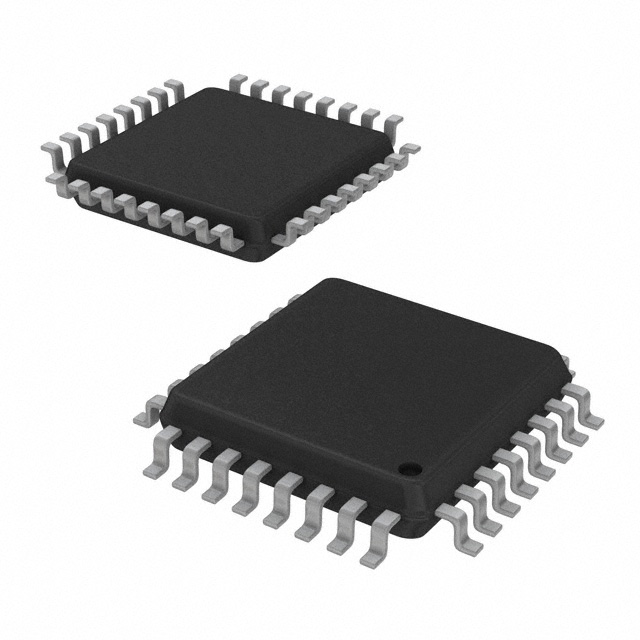
The NB3V8312CFAG is a high-performance clock buffer designed by onsemi, featuring a 1:12 fanout ratio and a maximum operating frequency of 250 MHz. This device is ideal for applications requiring efficient clock signal distribution with minimal skew and jitter. The NB3V8312CFAG supports a wide range of input and output voltage levels, making it versatile for various electronic systems. It is available in a 32-lead LQFP package, ensuring robust mechanical stability and thermal performance.
NB3V8312CFAG Features
- Fanout Ratio: 1:12, providing efficient distribution of clock signals to multiple destinations.
- Input and Output Types: Supports LVCMOS and LVTTL inputs, with LVCMOS outputs, ensuring compatibility with a wide range of digital circuits.
- Wide Supply Voltage Range: Operates from 1.6V to 3.465V, making it suitable for both low-power and standard voltage applications.
- High Frequency Performance: Capable of operating up to 250 MHz, ensuring high-speed signal integrity.
- Surface Mount Technology: Designed for surface mount applications, facilitating automated assembly processes and compact PCB designs.
- Compliance and Standards: REACH Unaffected and ROHS3 Compliant, ensuring environmental and regulatory compliance.
- Moisture Sensitivity Level: MSL 2 (1 Year), suitable for standard manufacturing environments.
- Package Type: Available in a 32-lead LQFP package, offering excellent thermal performance and mechanical robustness.
NB3V8312CFAG Applications
The NB3V8312CFAG is well-suited for a variety of applications where reliable clock signal distribution is critical. Some specific use cases include:
- Telecommunications: Ideal for distributing clock signals in base stations and network equipment.
- Computing: Suitable for server and workstation motherboards requiring high-speed clock distribution.
- Consumer Electronics: Applicable in high-definition tele andvisions multimedia devices where precise timing is essential.
- Industrial Control Systems: Provides reliable clock distribution in automation and control systems.
- Automotive Electronics: Ensures accurate clock signal distribution in advanced driver-assistance systems (ADAS) and infotainment systems.
Conclusion of NB3V8312CFAG
The NB3V8312CFAG from onsemi is a versatile and high-performance clock buffer that offers significant advantages in clock signal distribution. Its wide operating voltage range, high-frequency performance, and compatibility with various digital signal standards make it a reliable choice for a broad range of applications. The device's compliance with environmental and regulatory standards, along with its robust packaging, ensures long-term reliability and ease of integration into modern electronic designs. Whether in telecommunications, computing, or consumer electronics, the NB3V8312CFAG stands out as a superior solution for efficient and reliable clock signal distribution.
Tech Specifications
NB3V8312CFAG Documents
Download datasheets and manufacturer documentation for NB3V8312CFAG
General Announcement - 2D Barcoding (PDF) Temporary Suspension of ISO 9001 Certification for Hitachi Chemical Co., Ltd. INITIAL PRODUCT / PROCESS CHANGE NOTIFICATION (PDF) Final Product / Process Change Notification (PDF) Related Parts


Shopping Guide


.png?x-oss-process=image/format,webp/resize,h_32)


©2025 ERSA Electronics Corporation.