
 German
 Japanese
 Portuguese
 Korea
Korea
 Mexico
 Dutch
Dutch


onsemi
NCS20072DTBR2G

Why Choose Us?
Professional Platform
B2B & B2C purchasingDelivery at full speed
1-2 days deliveryWide variety
Original manufacturers365 days guarantee
Responsible quality
.png)


Tech Specifications
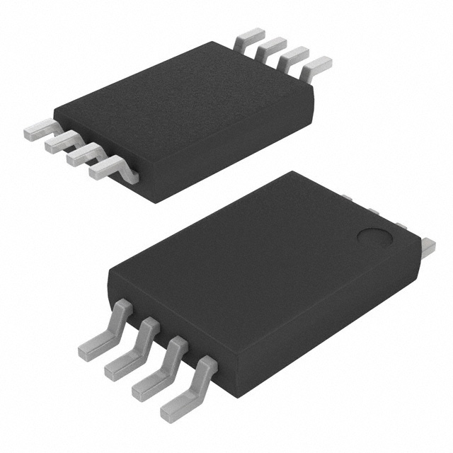
NCS20072DTBR2G Description
NCS20072DTBR2G Description
The NCS20072DTBR2G is a high-performance, dual-channel operational amplifier (op-amp) designed by ON Semiconductor. This device is part of the OP Amps, Buffer Amps ICs category and is offered in an 8-pin TSSOP package. With a wide supply voltage range of 2.7 V to 36 V, it is suitable for various applications that require low power consumption and high performance.
NCS20072DTBR2G Features
- Voltage - Supply Span (Max): 36 V
- Voltage - Supply Span (Min): 2.7 V
- Gain Bandwidth Product: 3.2 MHz
- Slew Rate: 2.4 V/µs
- Current - Input Bias: 5 pA
- Current - Supply: 420 µA (x2 Channels)
- Current - Output / Channel: 65 mA
- Voltage - Input Offset: 1.3 mV
- Mounting Type: Surface Mount
- Package: Tape & Reel (TR)
- Number of Circuits: 2
- REACH Status: REACH Unaffected
- RoHS Status: ROHS3 Compliant
- Moisture Sensitivity Level (MSL): 1 (Unlimited)
- ECCN: EAR99
- HTSUS: 8542.33.0001
- Amplifier Type: General Purpose
NCS20072DTBR2G Applications
The NCS20072DTBR2G is ideal for a variety of applications due to its high performance and versatility. Some specific use cases include:
- Audio Amplification: Its low input bias current and high slew rate make it suitable for audio applications where low noise and fast response are required.
- Sensor Conditioning: The wide supply voltage range and low input offset voltage make it an excellent choice for conditioning signals from sensors in industrial and automotive applications.
- Data Acquisition Systems: The device's high gain bandwidth product and low power consumption make it suitable for data acquisition systems in test and measurement equipment.
- Battery-Powered Devices: Its low power consumption and wide supply voltage range make it ideal for battery-powered devices, such as portable electronics and wearables.
Conclusion of NCS20072DTBR2G
The NCS20072DTBR2G is a versatile, dual-channel op-amp that offers high performance and low power consumption. Its wide supply voltage range, low input bias current, and high slew rate make it suitable for a variety of applications, including audio amplification, sensor conditioning, data acquisition systems, and battery-powered devices. With its REACH unaffected status and RoHS3 compliance, the NCS20072DTBR2G is an excellent choice for environmentally conscious designs.
FAQ
| Quantity | Unit Price | Ext. Price |
|---|---|---|
| 1+ | $0.45257 | $0.45 |
| 10+ | $0.44400 | $4.44 |
| 30+ | $0.43715 | $13.11 |
Not available to buy online? Want the lower wholesale price? Please Send RFQ to get best price, we will respond immediately


.png?x-oss-process=image/format,webp/resize,h_32)


