

onsemi
NLAS44599MNR2G
Analog Switches, Multiplexers, Demultiplexers

Not available to buy online? Want the lower wholesale price? Please Send RFQ to get best price, we will respond immediately


.png?x-oss-process=image/format,webp/resize,p_30)


NLAS44599MNR2G Description
NLAS44599MNR2G Description
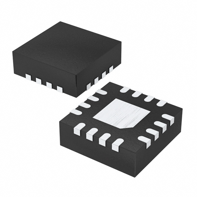
The NLAS44599MNR2G is a high-performance, dual-pole double-throw (DPDT) analog switch designed by onsemi. This device is part of the NLAS4 family and is known for its robust performance and versatility in various electronic applications. The NLAS44599MNR2G features a maximum on-state resistance of 25 ohms, ensuring minimal signal loss and high efficiency. It operates within a wide supply voltage range of 2V to 5.5V, making it suitable for a variety of power supply configurations. The switch is housed in a 16QFN package, which is ideal for surface-mount applications, providing a compact and reliable solution for space-constrained designs.
NLAS44599MNR2G Features
- Low Leakage Current: With a maximum leakage current of 10µA, the NLAS44599MNR2G ensures minimal power consumption and maintains signal integrity even in low-power applications.
- High Switching Speed: The device offers fast switching times of 14ns for turn-on and 5ns for turn-off, making it suitable for high-speed signal routing and processing.
- Low Channel Capacitance: The NLAS44599MNR2G has a channel capacitance of 10pF for both CS(off) and CD(off), which minimizes signal distortion and ensures high-frequency performance.
- Wide Bandwidth: The -3dB bandwidth of 175MHz allows for the transmission of wideband signals without significant attenuation.
- Charge Injection: The low charge injection of 3pC ensures minimal transient disturbances during switching, maintaining signal quality.
- Multiplexer/Demultiplexer Circuit: The 2:2 multiplexer/demultiplexer circuit provides efficient signal routing and switching capabilities.
- Moisture Sensitivity Level: With an MSL of 1 (Unlimited), the NLAS44599MNR2G is suitable for a wide range of environmental conditions, ensuring reliability and durability.
- Compliance: The device is REACH unaffected and classified under ECCN EAR99, ensuring compliance with international regulations and standards.
NLAS44599MNR2G Applications
The NLAS44599MNR2G is ideal for a variety of applications where high-speed signal switching and routing are required. Some specific use cases include:
- Telecommunications: High-speed data transmission and signal routing in communication systems.
- Consumer Electronics: Audio and video signal switching in multimedia devices such as TVs, set-top boxes, and gaming consoles.
- Industrial Control: Signal routing and switching in industrial automation and control systems.
- Medical Equipment: Signal processing and routing in medical imaging and diagnostic equipment.
- Automotive Electronics: Signal switching in automotive infotainment and control systems.
Conclusion of NLAS44599MNR2G
The NLAS44599MNR2G is a versatile and high-performance DPDT analog switch that offers significant advantages over similar models. Its low on-state resistance, fast switching times, and wide bandwidth make it an excellent choice for applications requiring high-speed signal routing and processing. The device's low leakage current and channel capacitance ensure minimal power consumption and signal distortion, while its compliance with international standards ensures reliability and durability. Although the NLAS44599MNR2G is now obsolete, it remains a benchmark for high-performance analog switches in the electronics industry.
Tech Specifications
NLAS44599MNR2G Documents
Download datasheets and manufacturer documentation for NLAS44599MNR2G
Related Parts


Shopping Guide


.png?x-oss-process=image/format,webp/resize,h_32)


©2025 ERSA Electronics Corporation.