
 German
 Japanese
 Portuguese
 Korea
Korea
 Mexico
 Dutch
Dutch


onsemi
NSS40301MDR2G

Why Choose Us?
Professional Platform
B2B & B2C purchasingDelivery at full speed
1-2 days deliveryWide variety
Original manufacturers365 days guarantee
Responsible quality
.png)


Tech Specifications
NSS40301MDR2G Description
NSS40301MDR2G Description
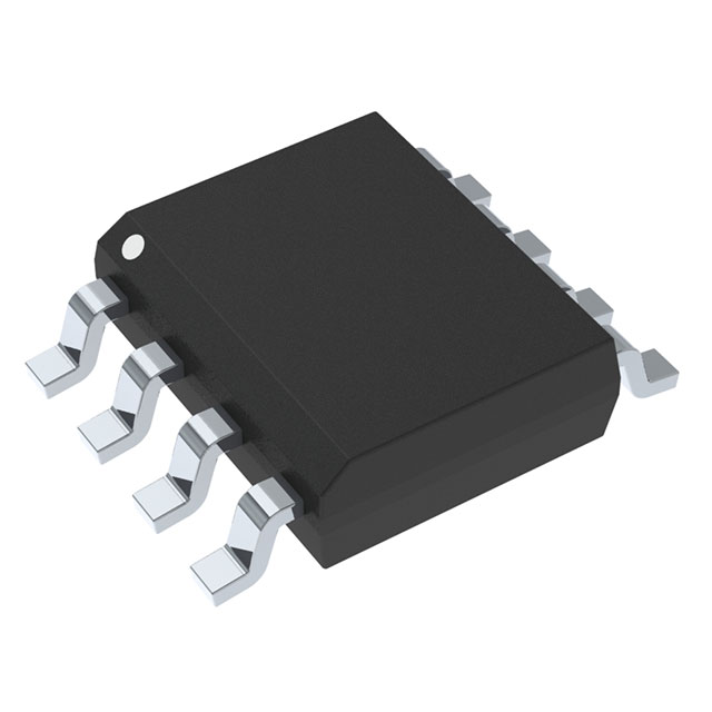
The NSS40301MDR2G is a high-performance dual NPN bipolar transistor array from ON Semiconductor, designed for applications requiring high current and voltage handling capabilities. This device is offered in an 8-pin SOIC package, making it suitable for surface-mount applications in a wide range of electronic systems. With its robust specifications and performance benefits, the NSS40301MDR2G is an ideal choice for power amplification, switching, and other demanding applications.
NSS40301MDR2G Features
- High Current Handling: The NSS40301MDR2G can handle a maximum collector current (Ic) of 3A, making it suitable for high-power applications.
- Low Saturation Voltage: The device features a low Vce saturation voltage of 115mV at 200mA and 2A, ensuring efficient operation in low-voltage applications.
- High Voltage Breakdown: With a maximum collector-emitter breakdown voltage of 40V, the NSS40301MDR2G can handle high-voltage applications with ease.
- High DC Current Gain: The device offers a minimum DC current gain (hFE) of 180 at 1A and 2V, providing excellent amplification capabilities.
- Surface Mount Packaging: The 8-pin SOIC package allows for surface-mount applications, enabling compact and efficient PCB layouts.
- RoHS Compliance: The NSS40301MDR2G is compliant with RoHS3 regulations, making it suitable for environmentally conscious designs.
NSS40301MDR2G Applications
The NSS40301MDR2G is ideal for a variety of applications where high current and voltage handling are required. Some specific use cases include:
- Power Amplifiers: The high current and voltage ratings make the NSS40301MDR2G suitable for use in power amplifiers, where high power output is needed.
- Switching Applications: The low saturation voltage and high current handling capabilities make this device ideal for switching applications, such as motor control and power distribution.
- Automotive Electronics: The NSS40301MDR2G can be used in automotive electronics, such as power windows, seat controls, and lighting systems, where high current and voltage ratings are essential.
- Industrial Control Systems: The device's robust specifications make it suitable for use in industrial control systems, where reliability and performance are critical.
Conclusion of NSS40301MDR2G
The NSS40301MDR2G is a versatile and high-performance dual NPN bipolar transistor array from ON Semiconductor. Its combination of high current handling, low saturation voltage, and high voltage breakdown capabilities make it an ideal choice for a wide range of applications, including power amplification, switching, and automotive electronics. With its RoHS compliance and surface-mount packaging, the NSS40301MDR2G is a reliable and environmentally conscious solution for demanding electronic systems.
FAQ
Not available to buy online? Want the lower wholesale price? Please Send RFQ to get best price, we will respond immediately


.png?x-oss-process=image/format,webp/resize,h_32)


