
 German
 Japanese
 Portuguese
 Korea
Korea
 Mexico
 Dutch
Dutch


onsemi
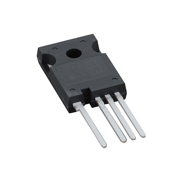
NTH4L028N170M1

Why Choose Us?
Professional Platform
B2B & B2C purchasingDelivery at full speed
1-2 days deliveryWide variety
Original manufacturers365 days guarantee
Responsible quality
.png)


Tech Specifications
NTH4L028N170M1 Description
NTH4L028N170M1 Description
The NTH4L028N170M1 is a high-performance Silicon Carbide (SiC) MOSFET from onsemi, designed for demanding applications that require high voltage and power handling capabilities. This device is currently in active production, ensuring ongoing availability and support. With a drain-to-source voltage (Vdss) of 1700V and a maximum power dissipation of 535W at Tc, it is well-suited for high-voltage applications.
NTH4L028N170M1 Features
- High Voltage Rating: The NTH4L028N170M1 boasts a 1700V drain-to-source voltage rating, making it ideal for applications that require high voltage handling.
- Low On-Resistance: With a maximum Rds(on) of 40mOhm at 60A and 20V, this device offers low on-resistance for efficient power dissipation.
- Silicon Carbide Technology: Leveraging SiC technology, the NTH4L028N170M1 provides superior performance in terms of switching speed and thermal management compared to traditional silicon-based MOSFETs.
- Robust Gate Charge: A maximum gate charge (Qg) of 200nC at 20V ensures efficient gate control and reduces switching losses.
- Compliance and Regulations: This device is REACH unaffected, RoHS3 compliant, and classified under ECCN EAR99, making it suitable for a wide range of applications without regulatory concerns.
NTH4L028N170M1 Applications
The NTH4L028N170M1 is ideal for applications that demand high voltage, power efficiency, and fast switching capabilities. Some specific use cases include:
- Industrial Motor Drives: The high voltage and low on-resistance make it suitable for motor control applications in industrial settings.
- Power Supplies: Its ability to handle high voltage and power makes it an excellent choice for power supply designs, particularly in renewable energy systems.
- Automotive Applications: The robustness and high voltage rating of the NTH4L028N170M1 make it suitable for electric and hybrid vehicle systems, including electric power steering and battery management.
Conclusion of NTH4L028N170M1
The NTH4L028N170M1 from onsemi stands out in the market due to its high voltage rating, low on-resistance, and SiC technology, which translates to superior performance and efficiency. Its compliance with various regulations and standards further enhances its appeal for a wide range of high-voltage applications. With its unique combination of features, the NTH4L028N170M1 is poised to deliver reliable and efficient performance in demanding environments.
FAQ
Not available to buy online? Want the lower wholesale price? Please Send RFQ to get best price, we will respond immediately


.png?x-oss-process=image/format,webp/resize,h_32)


