
 German
 Japanese
 Portuguese
 Korea
Korea
 Mexico
 Dutch
Dutch


onsemi
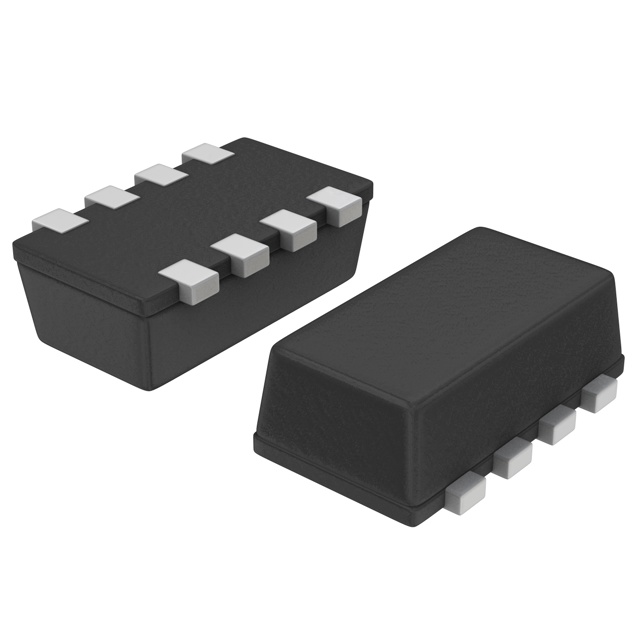
NTHD4508NT1G

Why Choose Us?
Professional Platform
B2B & B2C purchasingDelivery at full speed
1-2 days deliveryWide variety
Original manufacturers365 days guarantee
Responsible quality
.png)


Tech Specifications
NTHD4508NT1G Description
NTHD4508NT1G Description
The NTHD4508NT1G is a high-performance MOSFET (Metal Oxide) device manufactured by onsemi, designed for use in a variety of electronic applications. This 2N-channel device offers a drain to source voltage (Vdss) of 20V and can handle a continuous drain current (Id) of up to 3A at 25°C. With a maximum power dissipation of 1.13W, the NTHD4508NT1G is well-suited for applications requiring efficient power management.
NTHD4508NT1G Features
- Logic Level Gate: The NTHD4508NT1G features a logic level gate, enabling compatibility with standard logic level signals for easy integration into existing systems.
- Low Input Capacitance (Ciss): With a maximum input capacitance of 180pF at 10V, the NTHD4508NT1G offers fast switching speeds and reduced power consumption.
- Low Gate Charge (Qg): The device has a maximum gate charge of 4nC at 4.5V, contributing to its high-speed performance.
- Low Rds On: The NTHD4508NT1G boasts a low Rds On of 75mOhm at 3.1A and 4.5V, ensuring efficient power delivery.
- Surface Mount Technology: The device is designed for surface mount applications, allowing for compact and reliable integration into PCBs.
- ChipFET™ Package: The NTHD4508NT1G is available in the compact ChipFET™ package, which is ideal for space-constrained applications.
NTHD4508NT1G Applications
The NTHD4508NT1G is ideal for a variety of applications, including:
- Power Management: Due to its high voltage and current ratings, the NTHD4508NT1G is well-suited for power management applications in electronic devices.
- Automotive Electronics: The device's robust performance makes it suitable for use in automotive electronics, such as power windows and seat controls.
- Industrial Controls: The NTHD4508NT1G can be used in industrial control systems, where high voltage and current ratings are required.
- Telecommunications: The device's fast switching speeds and low power consumption make it ideal for telecommunications equipment.
Conclusion of NTHD4508NT1G
The NTHD4508NT1G is a versatile MOSFET device that offers a combination of high performance, low power consumption, and compatibility with standard logic level signals. Its unique features, such as low input capacitance and gate charge, make it an ideal choice for applications requiring fast switching speeds and efficient power management. However, it is important to note that the NTHD4508NT1G is now considered obsolete, which may limit its availability and suitability for new designs. Despite this, its robust performance and compact packaging make it a valuable option for existing systems and applications where high voltage and current ratings are required.
FAQ
Not available to buy online? Want the lower wholesale price? Please Send RFQ to get best price, we will respond immediately


.png?x-oss-process=image/format,webp/resize,h_32)


