

onsemi
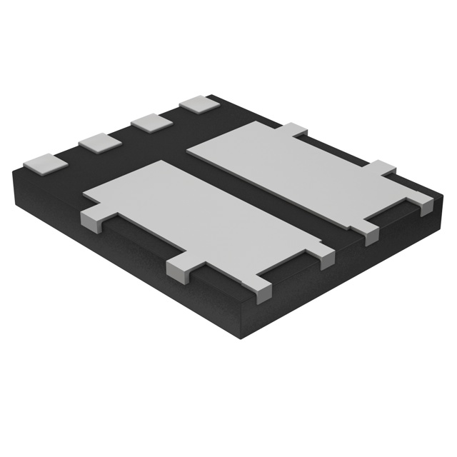
NVMFD5C478NLT1G
FET, MOSFET Arrays

Not available to buy online? Want the lower wholesale price? Please Send RFQ to get best price, we will respond immediately


.png?x-oss-process=image/format,webp/resize,p_30)


NVMFD5C478NLT1G Description
NVMFD5C478NLT1G Description
The NVMFD5C478NLT1G is a high-performance MOSFET from onsemi, designed for automotive applications. This 2N-channel MOSFET operates at a maximum drain-source voltage (Vdss) of 40V and can handle continuous drain currents (Id) of up to 10.5A at 25°C (Ta) and 29A at Tc. With a low on-resistance (Rds On) of 14.5mOhm at 7.5A and 10V, the NVMFD5C478NLT1G offers efficient power management in automotive systems.
NVMFD5C478NLT1G Features
- Technology: MOSFET (Metal Oxide) - Reliable and efficient power switching
- Grade: Automotive - Designed for demanding automotive environments
- Mounting Type: Surface Mount - Ideal for compact automotive electronics
- Input Capacitance (Ciss): 420pF @ 25V - Minimizes capacitive effects
- Gate Charge (Qg): 8.1nC @ 10V - Reduces switching losses
- Vgs(th): 2.2V @ 20µA - Ensures reliable threshold voltage
- Power - Max: 3.1W (Ta), 23W (Tc) - Supports high-power automotive applications
- Moisture Sensitivity Level (MSL): 1 (Unlimited) - Enhanced reliability in humid environments
- RoHS Status: ROHS3 Compliant - Environmentally friendly
- REACH Status: REACH Unaffected - Compliant with European chemical regulations
NVMFD5C478NLT1G Applications
The NVMFD5C478NLT1G is ideal for a variety of automotive applications, including:
- Power Management: Efficient power switching in automotive power systems
- Battery Management: Reliable voltage and current control in battery management systems
- Motor Control: Precise control of electric motors in electric vehicles (EVs) and hybrid electric vehicles (HEVs)
- LED Lighting: Efficient power management for automotive LED lighting systems
- Infotainment Systems: Reliable power switching for automotive infotainment systems
Conclusion of NVMFD5C478NLT1G
The NVMFD5C478NLT1G is a high-performance, automotive-grade MOSFET from onsemi, offering efficient power management and reliable operation in demanding automotive environments. With its low on-resistance, low gate charge, and high current handling capabilities, the NVMFD5C478NLT1G is an excellent choice for automotive power management, battery management, motor control, LED lighting, and infotainment systems. Its compliance with RoHS and REACH regulations makes it an environmentally friendly option for automotive electronics.
Tech Specifications
NVMFD5C478NLT1G Documents
Download datasheets and manufacturer documentation for NVMFD5C478NLT1G
NVMFD5C478NL MPN Label Update 08/Sep/2021 MPN label update 11/Oct/2021 NVMFD5C478NL onsemi RoHS onsemi REACH Material Declaration NVMFD5C478NLT1G Related Parts


Shopping Guide


.png?x-oss-process=image/format,webp/resize,h_32)


©2025 ERSA Electronics Corporation.