

onsemi
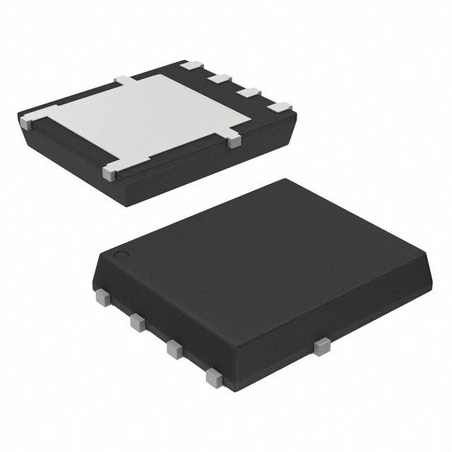
NVMFS5C406NT1G
Single FETs, MOSFETs

Not available to buy online? Want the lower wholesale price? Please Send RFQ to get best price, we will respond immediately


.png?x-oss-process=image/format,webp/resize,p_30)


NVMFS5C406NT1G Description
NVMFS5C406NT1G Description
The NVMFS5C406NT1G from onsemi is a high-performance N-channel MOSFET designed for demanding automotive and industrial applications. With a 40V drain-to-source voltage (Vdss) and an impressive continuous drain current (Id) of 52A (Ta) / 353A (Tc), this device delivers robust power handling in a compact 5DFN surface-mount package. It features an ultra-low on-resistance (Rds(on)) of just 0.8mΩ at 10V gate drive, ensuring minimal conduction losses and improved efficiency. The MOSFET is AEC-Q101 qualified, making it ideal for automotive systems where reliability under harsh conditions is critical.
NVMFS5C406NT1G Features
- Low Rds(on): 0.8mΩ @ 50A, 10V for reduced power dissipation.
- High Current Capability: Supports up to 353A (Tc) for high-power applications.
- Automotive Grade: Compliant with AEC-Q101, ensuring reliability in automotive environments.
- Optimized Gate Charge (Qg): 110nC @ 10V for fast switching and reduced switching losses.
- Wide Vgs Range: ±20V gate-to-source voltage tolerance for flexible drive requirements.
- Thermal Performance: 179W (Tc) power dissipation enables efficient heat management.
- RoHS3 & REACH Compliant: Environmentally friendly and suitable for global markets.
NVMFS5C406NT1G Applications
This MOSFET is ideal for high-efficiency power conversion and motor control applications, including:
- Automotive Systems: Electric power steering (EPS), 48V mild hybrid systems, and DC-DC converters.
- Industrial Power Supplies: High-current synchronous rectification and battery management systems (BMS).
- Motor Drives: Brushless DC (BLDC) and servo motor controllers requiring low Rds(on) and high thermal performance.
- Load Switches & OR-ing Circuits: Where low conduction loss and fast switching are critical.
Conclusion of NVMFS5C406NT1G
The NVMFS5C406NT1G stands out as a high-efficiency, automotive-grade MOSFET with exceptional current handling, ultra-low Rds(on), and superior thermal performance. Its 5DFN package ensures space savings without compromising power density, making it an excellent choice for automotive, industrial, and high-performance switching applications. With onsemi's proven reliability, this MOSFET is a top-tier solution for engineers seeking high power efficiency and rugged durability in demanding environments.
Tech Specifications
NVMFS5C406NT1G Documents
Download datasheets and manufacturer documentation for NVMFS5C406NT1G
Wafer Fab Capacity Expansion 14/Dec/2021 NVMFS5C406N MPN Label Update 08/Sep/2021 MPN label update 11/Oct/2021 NVMFS5C406N NVMFS5Cx0xN 27/Jul/2022 onsemi RoHS Material Declaration NVMFS5C406NT1G onsemi REACH Related Parts


Shopping Guide


.png?x-oss-process=image/format,webp/resize,h_32)


©2025 ERSA Electronics Corporation.