

onsemi
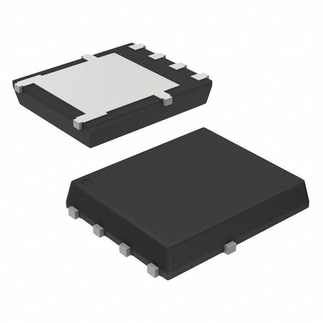
NVMFS5C604NLT1G
Single FETs, MOSFETs

Not available to buy online? Want the lower wholesale price? Please Send RFQ to get best price, we will respond immediately


.png?x-oss-process=image/format,webp/resize,p_30)


NVMFS5C604NLT1G Description
NVMFS5C604NLT1G Description
The NVMFS5C604NLT1G is a high-performance MOSFET (Metal Oxide) from onsemi, designed for automotive applications. This N-Channel device offers a drain-to-source voltage (Vdss) of 60V and can handle continuous drain currents of up to 40A at 25°C (Ta) and 287A at case temperature (Tc). With a maximum power dissipation of 3.9W at ambient temperature (Ta) and 200W at case temperature (Tc), it is suitable for demanding applications requiring high current and voltage capabilities.
NVMFS5C604NLT1G Features
- High Voltage and Current Ratings: The NVMFS5C604NLT1G boasts a 60V drain-to-source voltage and can handle up to 40A continuous drain current at 25°C, making it ideal for high-power applications.
- Low On-Resistance: With a maximum Rds On of 1.2mOhm at 50A and 10V, this MOSFET offers low conduction losses, improving efficiency in power management systems.
- Surface Mount Package: The 5DFN package allows for compact and efficient PCB layout, suitable for space-constrained automotive applications.
- Automotive Grade: Designed to meet the stringent requirements of automotive applications, ensuring reliability and durability in harsh environments.
- Compliance with Industry Standards: The NVMFS5C604NLT1G is REACH unaffected, RoHS3 compliant, and classified under ECCN EAR99, ensuring compliance with global regulations.
NVMFS5C604NLT1G Applications
The NVMFS5C604NLT1G is well-suited for a variety of automotive applications, including:
- Electric Vehicle (EV) Systems: Power management and control systems in electric and hybrid vehicles, where high voltage and current ratings are critical.
- Battery Management: Efficient battery charging and discharging circuits, benefiting from the low on-resistance and high current capabilities.
- Motor Control: High-power motor drives and control systems, leveraging the device's ability to handle large currents and voltages.
Conclusion of NVMFS5C604NLT1G
The NVMFS5C604NLT1G from onsemi is a robust and reliable MOSFET designed for high-performance automotive applications. Its combination of high voltage and current ratings, low on-resistance, and automotive-grade design make it an excellent choice for demanding power management and motor control systems. With compliance to industry standards and a compact surface-mount package, the NVMFS5C604NLT1G is a versatile solution for engineers looking to optimize performance and efficiency in their automotive designs.
Tech Specifications
NVMFS5C604NLT1G Documents
Download datasheets and manufacturer documentation for NVMFS5C604NLT1G
Wafer Fab 19/Feb/2021 NVMFS5C604NL NVMFS5C604NL NVMFS5Cx0xN 27/Jul/2022 T6 40V/60V Datasheet Update 30/Dec/2015 onsemi RoHS onsemi REACH Material Declaration NVMFS5C604NLT1G Related Parts


Shopping Guide


.png?x-oss-process=image/format,webp/resize,h_32)


©2025 ERSA Electronics Corporation.