

STMicroelectronics
TSV324IDT
OP Amps, Buffer Amps ICs
Not available to buy online? Want the lower wholesale price? Please Send RFQ to get best price, we will respond immediately


.png?x-oss-process=image/format,webp/resize,p_30)


TSV324IDT Description
TSV324IDT Description
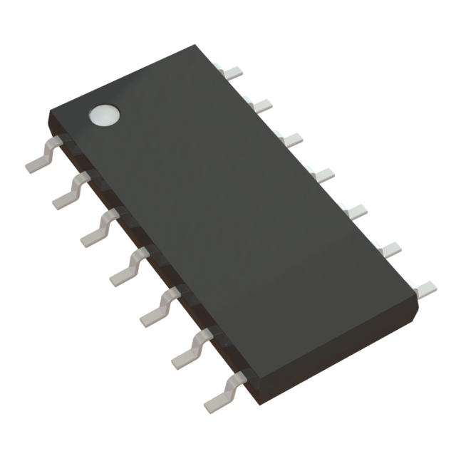
The TSV324IDT from STMicroelectronics is a general-purpose quad operational amplifier designed for automotive-grade applications, offering robust performance in a compact 14-pin SOIC package. This ROHS3-compliant and REACH-unaffected IC operates over a wide supply voltage range (2.5V to 6V), making it suitable for low-voltage and battery-powered systems. With a 1.4 MHz gain bandwidth product (GBW) and a slew rate of 0.6V/µs, it balances speed and power efficiency, drawing just 500µA per amplifier. Its low input bias current (70 nA) and minimal input offset voltage (200 µV) ensure precision in signal conditioning and sensor interfacing. Packaged in Tape & Reel (TR), it is optimized for high-volume surface-mount assembly.
TSV324IDT Features
- Automotive-Grade Reliability: Meets stringent automotive standards for durability and performance.
- Low Power Consumption: 500µA supply current per amplifier extends battery life in portable devices.
- High Output Drive: 80 mA output current enables direct driving of LEDs or small loads.
- Wide Supply Range: 2.5V to 6V operation supports diverse power architectures.
- Low Noise & Offset: 200 µV offset voltage and 70 nA bias current enhance signal fidelity.
- Compact Quad Configuration: Integrates four amplifiers in a space-saving 14SO package.
TSV324IDT Applications
- Automotive Systems: Sensor signal conditioning, ECU interfaces, and infotainment systems.
- Portable Electronics: Battery-powered devices requiring low quiescent current.
- Industrial Control: Precision instrumentation, PLCs, and low-voltage analog circuits.
- Consumer Electronics: Audio preamps, filter stages, and voltage followers.
- Medical Devices: Low-power signal amplification in wearable health monitors.
Conclusion of TSV324IDT
The TSV324IDT stands out as a versatile, low-power quad op-amp with automotive-grade robustness, making it ideal for harsh environments and energy-sensitive designs. Its balanced performance (1.4 MHz GBW, 0.6V/µs slew rate) and low-voltage operation cater to modern analog design needs, while its high output current expands usability beyond typical op-amp roles. For engineers seeking reliability, precision, and integration in a single package, the TSV324IDT is a compelling choice.
Tech Specifications
TSV324IDT Documents
Download datasheets and manufacturer documentation for TSV324IDT
 TSV321(A), 358(A), 324(A) TSV324 View All Specifications TSV321(A), 358(A), 324(A)
 Related Parts


Shopping Guide


.png?x-oss-process=image/format,webp/resize,h_32)


©2025 ERSA Electronics Corporation.