
 German
 Japanese
 Portuguese
 Korea
Korea
 Mexico
 Dutch
Dutch


STMicroelectronics
TSX922IYDT

Why Choose Us?
Professional Platform
B2B & B2C purchasingDelivery at full speed
1-2 days deliveryWide variety
Original manufacturers365 days guarantee
Responsible quality
.png)


Tech Specifications
TSX922IYDT Description
TSX922IYDT Description
The TSX922IYDT is a high-performance, automotive-grade operational amplifier (op-amp) from STMicroelectronics, designed for demanding applications that require precision and reliability. This dual-channel CMOS op-amp offers a wide supply voltage range of 4V to 16V, making it suitable for various power supply configurations. With a gain bandwidth product of 10 MHz and a slew rate of 17V/µs, the TSX922IYDT delivers excellent high-frequency performance and fast response times.
TSX922IYDT Features
- Wide Supply Voltage Range: The TSX922IYDT operates over a supply voltage range of 4V to 16V, providing flexibility in power supply design.
- High Gain Bandwidth Product: A gain bandwidth product of 10 MHz ensures excellent high-frequency performance for demanding applications.
- Fast Slew Rate: The 17V/µs slew rate enables rapid response times, making the TSX922IYDT suitable for high-speed signal processing.
- Low Input Bias Current: The 10 pA input bias current minimizes the loading effect on the input signal, ensuring accurate signal processing.
- Low Input Offset Voltage: The 5 mV input offset voltage contributes to the op-amp's high accuracy and precision.
- Automotive Grade: The TSX922IYDT is designed to meet the stringent requirements of automotive applications, ensuring reliability and durability in harsh environments.
- RoHS Compliance: The TSX922IYDT is compliant with RoHS3 regulations, making it suitable for environmentally friendly designs.
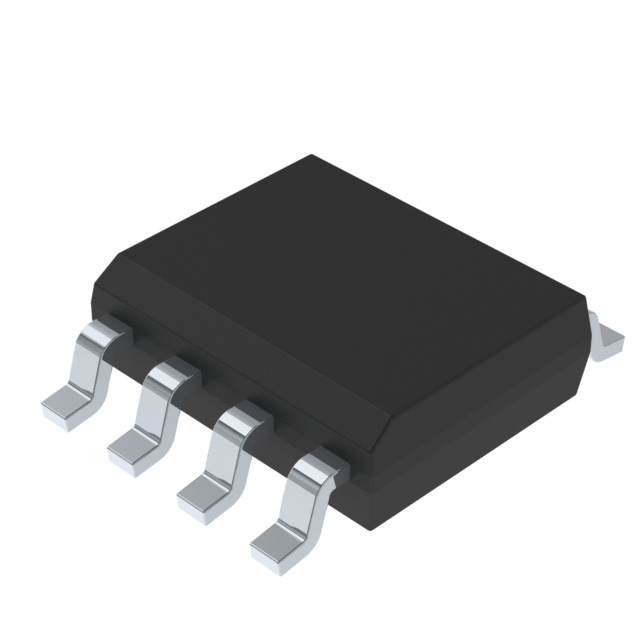
- Surface Mount Packaging: The TSX922IYDT is available in an 8-pin SOIC package,,。
TSX922IYDT Applications
The TSX922IYDT is ideal for a variety of applications where high performance, reliability, and precision are critical:
- Automotive Systems: Due to its automotive-grade rating, the TSX922IYDT is well-suited for use in automotive control systems, such as engine control units (ECUs) and sensor interfaces.
- Industrial Control: The TSX922IYDT's robust performance makes it suitable for industrial control applications, including motor control and process monitoring.
- Audio and Video Processing: The high slew rate and low distortion characteristics of the TSX922IYDT make it an excellent choice for audio and video signal processing applications.
- Sensor Conditioning: The low input bias current and low noise of the TSX922IYDT make it ideal for conditioning signals from precision sensors in various applications.
Conclusion of TSX922IYDT
The TSX922IYDT from STMicroelectronics is a versatile, high-performance op-amp designed for demanding automotive and industrial applications. Its wide supply voltage range, high gain bandwidth product, and low input bias current make it an excellent choice for precision signal processing. With its automotive-grade rating and RoHS compliance, the TSX922IYDT is a reliable and environmentally friendly solution for a wide range of applications.
FAQ
Not available to buy online? Want the lower wholesale price? Please Send RFQ to get best price, we will respond immediately


.png?x-oss-process=image/format,webp/resize,h_32)


