

STMicroelectronics
TSV612AIDT
OP Amps, Buffer Amps ICs

Not available to buy online? Want the lower wholesale price? Please Send RFQ to get best price, we will respond immediately


.png?x-oss-process=image/format,webp/resize,p_30)


TSV612AIDT Description
TSV612AIDT Description
The TSV612AIDT is a high-performance, dual-channel operational amplifier (op-amp) from STMicroelectronics. This CMOS op-amp offers a wide supply voltage range of 1.5V to 5.5V, making it suitable for a variety of low-voltage applications. With a gain bandwidth product of 120 kHz and a slew rate of 0.04V/µs, the TSV612AIDT delivers excellent speed and stability for demanding signal processing tasks.
TSV612AIDT Features
- Low Input Bias Current: The TSV612AIDT boasts an ultra-low input bias current of 1 pA, which is crucial for maintaining signal integrity in high-impedance applications.
- Low Voltage Operation: The op-amp can operate with supply voltages as low as 1.5V, making it ideal for battery-powered devices and other low-power applications.
- High Gain Bandwidth Product: The 120 kHz gain bandwidth product ensures fast response times and stability in high-frequency applications.
- Low Input Offset Voltage: The 800 µV input offset voltage provides excellent accuracy and linearity in precision applications.
- Low Supply Current: The TSV612AIDT consumes only 10.5 µA of supply current, contributing to low-power consumption in battery-operated devices.
- Robust Output Current: Each channel can deliver up to 63 mA of output current, making it suitable for driving capacitive loads and other demanding applications.
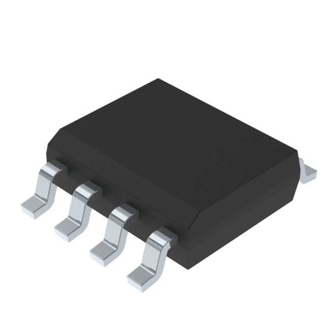
- Surface Mount Packaging: The TSV612AIDT is available in an 8-pin SOIC package, which is ideal for surface-mount applications in PCB designs.
TSV612AIDT Applications
The TSV612AIDT is well-suited for a wide range of applications due to its combination of low power consumption, low input bias current, and high performance:
- Portable Electronics: The low supply voltage and low power consumption make it ideal for battery-powered devices such as smartphones, tablets, and wearables.
- Precision Instruments: The low input bias current and low input offset voltage make it suitable for precision measurement and control applications in scientific instruments and industrial equipment.
- Audio Applications: The high slew rate and low distortion characteristics make it suitable for audio preamplifiers and signal conditioning circuits in consumer electronics.
- Automotive Systems: The TSV612AIDT can be used in automotive sensor interfaces, infotainment systems, and control modules due to its robust performance and low power consumption.
Conclusion of TSV612AIDT
The TSV612AIDT is a versatile and high-performance dual-channel op-amp from STMicroelectronics. Its unique combination of low power consumption, low input bias current, and high gain bandwidth product make it an excellent choice for a wide range of applications, including portable electronics, precision instruments, audio equipment, and automotive systems. With its robust performance and low power consumption, the TSV612AIDT is a reliable and cost-effective solution for demanding signal processing tasks.
Tech Specifications
TSV612AIDT Documents
Download datasheets and manufacturer documentation for TSV612AIDT
PROCESS CHANGE NOTIFICATION (PDF) Product Change Notification (PDF) Related Parts


Shopping Guide


.png?x-oss-process=image/format,webp/resize,h_32)


©2025 ERSA Electronics Corporation.