

STMicroelectronics
TS272BIDT
OP Amps, Buffer Amps ICs
Not available to buy online? Want the lower wholesale price? Please Send RFQ to get best price, we will respond immediately


.png?x-oss-process=image/format,webp/resize,p_30)


TS272BIDT Description
TS272BIDT Description
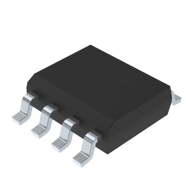
The TS272BIDT from STMicroelectronics is a high-performance, dual-channel CMOS operational amplifier designed for precision analog applications. Operating within a 3V to 16V supply range, it delivers a 3.5 MHz gain bandwidth product and a 5.5V/µs slew rate, making it suitable for high-speed signal conditioning. With an ultra-low 1 pA input bias current and 250 µV input offset voltage, it ensures accuracy in sensitive circuits. Packaged in an 8-SOIC and available in Tape & Reel (TR), it is optimized for surface-mount assembly. The device is ROHS3 compliant, REACH unaffected, and rated for MSL 1 (Unlimited) reliability.
TS272BIDT Features
- Dual-Channel CMOS Design: Two independent amplifiers in one package, reducing board space.
- Wide Supply Range (3V–16V): Supports both low-voltage and industrial-level applications.
- Low Power Consumption: 1mA per channel supply current enhances energy efficiency.
- High Output Drive (45 mA/channel): Capable of driving heavy loads, such as ADCs or transmission lines.
- Ultra-Low Input Bias (1 pA): Ideal for high-impedance sensor interfaces (e.g., photodiodes, piezoelectric sensors).
- Fast Slew Rate (5.5V/µs): Minimizes distortion in high-frequency signals.
TS272BIDT Applications
- Portable Electronics: Battery-powered devices benefit from its low-voltage operation and minimal power draw.
- Signal Conditioning: Precision amplification for strain gauges, thermocouples, and medical sensors.
- Active Filters: High GBW and slew rate enable stable performance in audio and RF filtering.
- Data Acquisition Systems: Low offset and bias current ensure accuracy in ADC/DAC interfaces.
- Industrial Control: Robust performance in motor control loops and instrumentation amplifiers.
Conclusion of TS272BIDT
The TS272BIDT stands out for its low-noise CMOS architecture, wide voltage range, and high output drive, making it a versatile choice for precision and high-speed analog designs. Its dual-channel integration and surface-mount compatibility further streamline system design. Engineers targeting sensor interfaces, portable systems, or industrial controls will find this amplifier a reliable, high-performance solution.
Tech Specifications
TS272BIDT Documents
Download datasheets and manufacturer documentation for TS272BIDT
 TS272C,I,M Box Label Chg 28/Jul/2016 TS272 View All Specifications TS272C,I,M
 Related Parts


Shopping Guide


.png?x-oss-process=image/format,webp/resize,h_32)


©2025 ERSA Electronics Corporation.