

STMicroelectronics
TSV633AIST
OP Amps, Buffer Amps ICs

Not available to buy online? Want the lower wholesale price? Please Send RFQ to get best price, we will respond immediately


.png?x-oss-process=image/format,webp/resize,p_30)


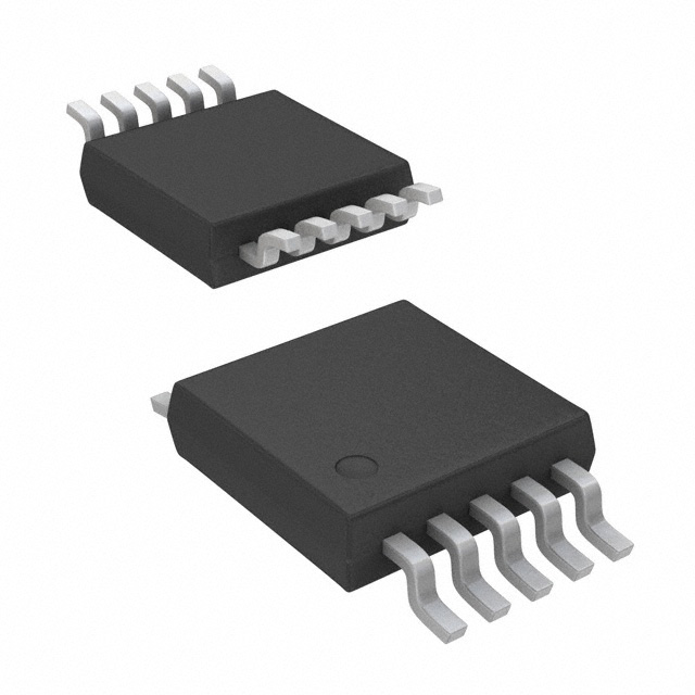
TSV633AIST Description
TSV633AIST Description
The TSV633AIST from STMicroelectronics is a general-purpose operational amplifier (op-amp) designed for automotive-grade applications, offering a balance of low power consumption and high performance. Packaged in a 10-MiniSO format with tape & reel (TR) mounting, it features dual-channel circuitry (2 circuits) and operates across a wide supply voltage range of 1.5V to 5.5V, making it versatile for battery-powered and low-voltage systems. With ROHS3 compliance and REACH unaffected status, it meets stringent environmental and automotive reliability standards.
TSV633AIST Features
- Ultra-Low Power: Consumes only 50µA per channel, ideal for energy-sensitive designs.
- High Precision: Input offset voltage of 800µV and input bias current of 1pA ensure accuracy in signal conditioning.
- Bandwidth & Speed: 880kHz gain bandwidth product (GBW) and 0.34V/µs slew rate for stable performance in dynamic applications.
- Robust Output: Delivers 74mA output current per channel, supporting moderate load-driving tasks.
- Automotive-Grade: AEC-Q100 qualified for harsh environments (temperature, vibration, etc.).
- Miniaturized Packaging: 10-MiniSO saves board space in compact designs.
TSV633AIST Applications
- Sensor Interfaces: Ideal for piezoelectric, pressure, or temperature sensors due to low noise and bias current.
- Battery-Powered Systems: Portable medical devices, IoT nodes, and energy harvesters benefit from its low quiescent current.
- Active Filtering: Suitable for audio and signal processing with its balanced GBW and slew rate.
- Automotive Electronics: ECUs, infotainment systems, and ADAS sensors leverage its ruggedized design.
Conclusion of TSV633AIST
The TSV633AIST stands out as a high-efficiency, precision op-amp tailored for automotive and portable electronics. Its low-voltage operation, minimal power draw, and robust performance make it superior to generic op-amps in noise-critical and space-constrained applications. Engineers seeking reliable amplification in harsh or power-limited environments will find this IC an optimal solution.
Tech Specifications
TSV633AIST Documents
Download datasheets and manufacturer documentation for TSV633AIST
TSV63x(A) Moisture Barrier Bag 09/May/2016 TSV633A View All Specifications TSV63x(A) Related Parts


Shopping Guide


.png?x-oss-process=image/format,webp/resize,h_32)


©2025 ERSA Electronics Corporation.