
 German
 Japanese
 Portuguese
 Korea
Korea
 Mexico
 Dutch
Dutch


Texas Instruments
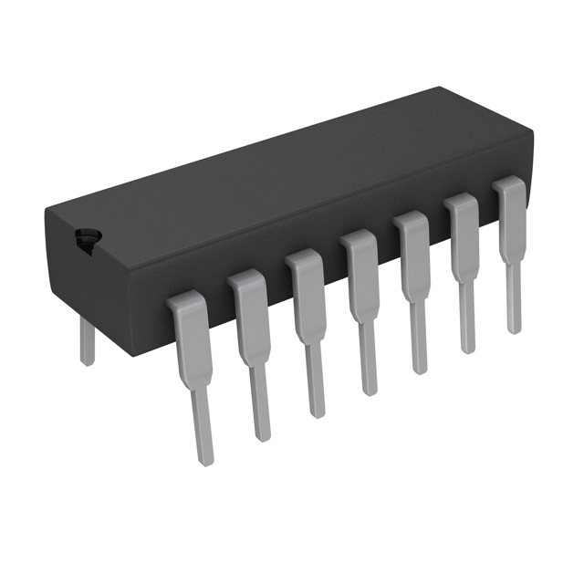
CD40106BE

Why Choose Us?
Professional Platform
B2B & B2C purchasingDelivery at full speed
1-2 days deliveryWide variety
Original manufacturers365 days guarantee
Responsible quality
.png)


Tech Specifications
CD40106BE Description
The Texas Instruments CD40106BE is a high-performance hex inverter buffer and line driver integrated circuit (IC). It is part of the 74HCxx series of digital logic devices and is designed for use in a variety of applications that require high-speed, low-power operation.
Description:
The CD40106BE is a 16-pin package that contains six independent inverter buffers. Each buffer is capable of driving up to 10 TTL loads and has a high output current drive capability. The device is designed to operate over a wide range of supply voltages (2V to 6V) and a wide temperature range (-40°C to +85°C).
Features:
- Hex inverter buffer and line driver
- 16-pin package
- High-speed operation
- Low-power consumption
- Wide supply voltage range (2V to 6V)
- Wide temperature range (-40°C to +85°C)
- Capable of driving up to 10 TTL loads
- High output current drive capability
- Compatible with TTL and CMOS logic families
Applications:
The CD40106BE is suitable for a wide range of applications, including but not limited to:
- Digital signal processing
- Data communication systems
- High-speed data buses
- Buffering and level conversion between TTL and CMOS logic families
- Memory address and data line drivers
- Counter and register applications
- Glitch suppression in digital systems
- Driving relays, solenoids, and other high-current loads
The CD40106BE is a versatile and reliable device that can be used in various digital logic applications requiring high-speed operation and low-power consumption. Its compatibility with both TTL and CMOS logic families makes it a popular choice for designers working with mixed-signal systems.
FAQ
| Quantity | Unit Price | Ext. Price |
|---|---|---|
| 10+ | $0.46457 | $4.65 |
| 25+ | $0.40285 | $10.07 |
| 100+ | $0.34115 | $34.12 |
| 500+ | $0.31372 | $156.86 |
| 1000+ | $0.29657 | $296.57 |
Not available to buy online? Want the lower wholesale price? Please Send RFQ to get best price, we will respond immediately


.png?x-oss-process=image/format,webp/resize,h_32)


