
Texas Instruments
CD40107BM
Gates and Inverters


.png?x-oss-process=image/format,webp/resize,p_30)


CD40107BM Description
CD40107BM Description
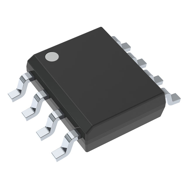
The CD40107BM is a high-performance NAND gate Logic IC chip designed for a wide range of digital applications. Manufactured by Texas Instruments, this device is part of the 4000B series and is known for its robustness and versatility. The CD40107BM features a maximum propagation delay of 100ns at 15V with a load capacitance of 50pF, ensuring fast and reliable signal processing. It operates within a supply voltage range of 3V to 18V, making it suitable for various power supply configurations.
This IC is designed with a surface-mount package, specifically in an 8SOIC format, which allows for easy integration into modern printed circuit boards. The CD40107BM supports an input logic level of 1.5V to 4V for low signals and 3.5V to 11V for high signals, providing flexibility in interfacing with different digital systems. Additionally, it features open-drain outputs, which can be advantageous in certain circuit designs requiring pull-up resistors for signal integrity.
CD40107BM Features
- Logic Type: NAND Gate
- Number of Circuits: 2
- Number of Inputs per Circuit: 2
- Voltage - Supply: 3V to 18V
- Max Propagation Delay: 100ns @ 15V, 50pF
- Input Logic Level - Low: 1.5V to 4V
- Input Logic Level - High: 3.5V to 11V
- Current - Quiescent (Max): 4 µA
- Features: Open Drain
- Package: Tube
- Mounting Type: Surface Mount
- Moisture Sensitivity Level (MSL): 1 (Unlimited)
- ECCN: EAR99
- HTSUS: 8542.39.0001
- REACH Status: REACH Unaffected
- RoHS Status: ROHS3 Compliant
CD40107BM Applications
The CD40107BM is ideal for applications requiring high-speed digital signal processing and low power consumption. Its wide operating voltage range and open-drain feature make it suitable for a variety of digital systems, including:
- Consumer Electronics: Used in devices where low power and high performance are critical, such as smartphones, tablets, and digital cameras.
- Automotive Electronics: Ideal for automotive applications due to its robustness and ability to operate within a wide voltage range.
- Industrial Control Systems: Suitable for control systems that require reliable and fast digital signal processing.
- Communication Systems: Used in communication devices where signal integrity and low power consumption are essential.
Conclusion of CD40107BM
The CD40107BM is a versatile and high-performance NAND gate Logic IC chip that offers significant advantages over similar models. Its wide operating voltage range, low quiescent current, and open-drain feature make it an ideal choice for a variety of applications. The device's fast propagation delay and surface-mount package ensure easy integration and reliable performance in modern electronic systems. With its compliance to industry standards such as REACH and RoHS3, the CD40107BM is a reliable and environmentally friendly solution for digital circuit design.
Tech Specifications
CD40107BM Documents
Download datasheets and manufacturer documentation for CD40107BM
 Mult Dev Wafer Fab Site 22/Dec/2023
  CD40107B Types
  CD40107B Types
  Design 25/Feb/2022 Mult Dev 27/Jul/2023
 Shopping Guide


.png?x-oss-process=image/format,webp/resize,h_32)


