

Texas Instruments
CD4010BM
Buffers, Drivers, Receivers, Transceivers

Not available to buy online? Want the lower wholesale price? Please Send RFQ to get best price, we will respond immediately


.png?x-oss-process=image/format,webp/resize,p_30)


CD4010BM Description
CD4010BM Description
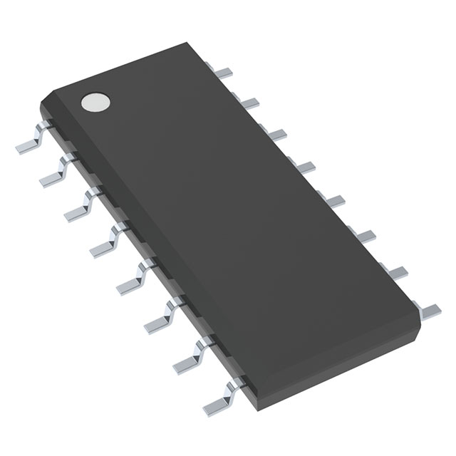
The CD4010BM from Texas Instruments is a hex non-inverting buffer belonging to the 4000B series, designed for surface-mount applications. This ROHS3 Compliant IC operates over a wide voltage range of 3V to 18V, making it versatile for both low and high-voltage logic systems. Packaged in a 16-SOIC tube, it features six independent buffers (1-bit per element), ensuring reliable signal conditioning and level shifting. With a high output current capability (3mA source, 36mA sink), it efficiently drives capacitive or resistive loads, making it ideal for interfacing between different logic families.
CD4010BM Features
- Wide Supply Voltage Range (3V–18V): Supports compatibility with TTL, CMOS, and other logic levels.
- High Output Drive (3mA/36mA): Ensures robust signal integrity in noisy environments.
- Low Power Consumption: Optimized for energy-efficient designs.
- Six Independent Buffers: Enables parallel signal processing with minimal crosstalk.
- Surface-Mount (16-SOIC): Saves PCB space while maintaining durability.
- MSL 1 (Unlimited Shelf Life): Suitable for extended storage without moisture sensitivity concerns.
- REACH Unaffected & EAR99: Compliant with global environmental and export regulations.
CD4010BM Applications
The CD4010BM excels in:
- Logic Level Shifting: Bridging 5V TTL and 3.3V CMOS systems.
- Signal Buffering: Isolating sensitive circuits from load-induced distortions.
- Clock Distribution Networks: Maintaining signal fidelity in timing-critical applications.
- Industrial Control Systems: Withstanding voltage fluctuations in harsh environments.
- Consumer Electronics: Power management and I/O interfacing in portable devices.
Conclusion of CD4010BM
The CD4010BM stands out for its robust performance, flexibility, and reliability in diverse digital systems. Its high noise immunity, wide voltage range, and strong output drive make it superior to basic buffers, while its compact SOIC package suits modern high-density designs. Whether for industrial automation, consumer tech, or embedded systems, this IC delivers consistent performance, backed by Texas Instruments' quality assurance. A strategic choice for engineers prioritizing efficiency, compliance, and scalability.
Tech Specifications
CD4010BM Documents
Download datasheets and manufacturer documentation for CD4010BM
CD4009UB,10B Types CD4009UB,10B Types Related Parts


Shopping Guide


.png?x-oss-process=image/format,webp/resize,h_32)


©2025 ERSA Electronics Corporation.