
 German
 Japanese
 Portuguese
 Korea
Korea
 Mexico
 Dutch
Dutch


Texas Instruments
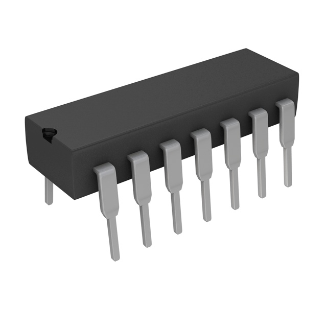
CD4012BE

Why Choose Us?
Professional Platform
B2B & B2C purchasingDelivery at full speed
1-2 days deliveryWide variety
Original manufacturers365 days guarantee
Responsible quality
.png)


Tech Specifications
CD4012BE Description
CD4012BE Description
The CD4012BE is a high-performance NAND gate integrated circuit (IC) designed and manufactured by Texas Instruments. This device is part of the 4000B series and is offered in a 14-pin dual in-line package (DIP). It features a maximum propagation delay of 90ns at 15V and 50pF, making it suitable for applications requiring fast switching times. The CD4012BE operates over a wide supply voltage range of 3V to 18V, providing flexibility in various electronic systems.
CD4012BE Features
- Logic Type: NAND Gate - The CD4012BE is a 4-input NAND gate, offering high-density logic functionality in a compact package.
- Max Propagation Delay: 90ns @ 15V, 50pF - This fast switching time makes the CD4012BE ideal for high-speed applications.
- Voltage - Supply: 3V ~ 18V - The wide operating voltage range allows for compatibility with various power sources.
- Input Logic Levels: Low (1.5V ~ 4V) and High (3.5V ~ 11V) - These levels ensure reliable operation across different input voltages.
- Current - Quiescent (Max): 1 µA - The low quiescent current contributes to energy efficiency in power-sensitive applications.
- Current - Output High, Low: 3.4mA, 3.4mA - These output currents provide sufficient drive capability for various loads.
- RoHS Status: ROHS3 Compliant - The CD4012BE meets environmental regulations, making it suitable for eco-friendly designs.
- Mounting Type: Through Hole - This mounting type ensures reliable mechanical and electrical connections in PCB designs.
CD4012BE Applications
The CD4012BE is ideal for various applications due to its high-speed performance, wide voltage range, and low power consumption. Some specific use cases include:
- Digital Logic Circuits: The CD4012BE can be used to create complex digital logic functions, such as decoders, encoders, and multiplexers.
- Signal Processing: Its fast switching time makes it suitable for signal processing applications, such as filters and mixers.
- Automotive Electronics: The CD4012BE can be used in automotive control systems, where high reliability and low power consumption are critical.
- Telecommunications: The device's wide voltage range and low quiescent current make it suitable for power-sensitive telecommunication equipment.
Conclusion of CD4012BE
The CD4012BE is a versatile NAND gate IC that offers a combination of high performance, wide voltage range, and low power consumption. Its unique features, such as fast propagation delay and low quiescent current, make it an excellent choice for a variety of applications, including digital logic circuits, signal processing, automotive electronics, and telecommunications. With its RoHS compliance and wide operating voltage range, the CD4012BE is a reliable and eco-friendly solution for modern electronic designs.
FAQ
| Quantity | Unit Price | Ext. Price |
|---|---|---|
| 1+ | $0.67760 | $0.68 |
| 10+ | $0.48576 | $4.86 |
| 25+ | $0.43648 | $10.91 |
| 100+ | $0.38271 | $38.27 |
| 250+ | $0.35700 | $89.25 |
Not available to buy online? Want the lower wholesale price? Please Send RFQ to get best price, we will respond immediately


.png?x-oss-process=image/format,webp/resize,h_32)


