
Texas Instruments
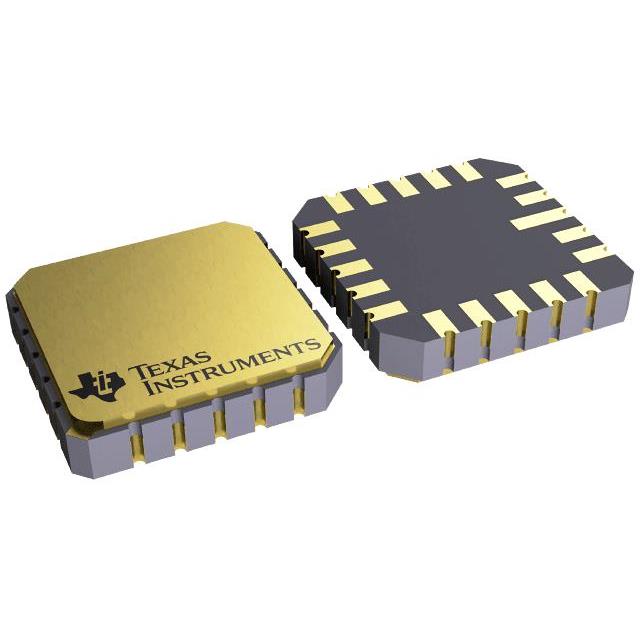
CD4013BF
Flip Flops


.png?x-oss-process=image/format,webp/resize,p_30)


CD4013BF Description
CD4013BF Description
The CD4013BF, manufactured by Texas Instruments, is a high-performance flip-flop integrated circuit that belongs to the 4000B series. This dual 1-bit D-type flip-flop offers a range of features that cater to various electronic applications. With a clock frequency of 24 MHz, it operates efficiently within a supply voltage range of 3V to 18V. The device is designed to provide a maximum propagation delay of 90ns at 15V and 50pF, ensuring quick response times. The quiescent current is a low 20 µA, contributing to energy efficiency.
CD4013BF Features
- High Clock Frequency: The CD4013BF supports a clock frequency of up to 24 MHz, making it suitable for high-speed applications.
- Low Propagation Delay: At 90ns, the propagation delay is minimal, ensuring fast switching times.
- Low Quiescent Current: With a quiescent current of only 20 µA, the CD4013BF is energy-efficient.
- Complementary Outputs: The flip-flop provides complementary outputs, which can be beneficial in reducing noise and improving signal integrity.
- Positive Edge Trigger: The device is triggered on the positive edge of the clock signal, simplifying timing control in digital circuits.
- Through Hole Mounting: The through-hole package facilitates easy integration into existing PCB designs.
- Dual Elements: The CD4013BF includes two D-type flip-flops, doubling the functionality in a single package.
- Set and Reset Functions: Each flip-flop has individual set and reset capabilities, offering flexibility in circuit design.
- RoHS Compliance: The CD4013BF is compliant with RoHS3 standards, making it an environmentally friendly choice.
CD4013BF Applications
The CD4013BF is ideal for a variety of applications where reliable and fast data storage and retrieval are required. Some specific use cases include:
- Digital Clocks and Timers: The high-speed operation and low power consumption make it suitable for digital clock and timer circuits.
- Data Storage in Computers: In computer systems, the CD4013BF can be used for temporary data storage in memory circuits.
- Communication Systems: The device's fast edge-triggered operation is beneficial in communication systems for signal synchronization.
- Automotive Electronics: Due to its robustness and reliability, the CD4013BF can be used in automotive electronics for various control and timing functions.
Conclusion of CD4013BF
The CD4013BF from Texas Instruments stands out for its combination of high-speed operation, low power consumption, and dual functionality in a single package. Its positive edge-triggered operation and complementary outputs make it a versatile choice for a wide range of digital applications. With its RoHS compliance and active product status, the CD4013BF is a reliable option for designers looking to incorporate high-performance flip-flops into their next project.
Tech Specifications
CD4013BF Documents
Download datasheets and manufacturer documentation for CD4013BF
 CD4013B
 Shopping Guide


.png?x-oss-process=image/format,webp/resize,h_32)


