
 German
 Japanese
 Portuguese
 Korea
Korea
 Mexico
 Dutch
Dutch


Texas Instruments
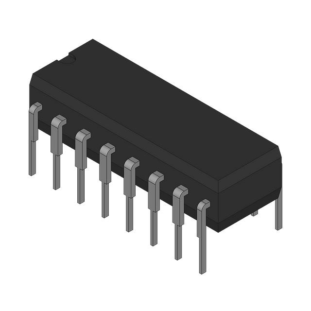
CD40175BNS

Why Choose Us?
Professional Platform
B2B & B2C purchasingDelivery at full speed
1-2 days deliveryWide variety
Original manufacturers365 days guarantee
Responsible quality
.png)


Tech Specifications
CD40175BNS Description
CD40175BNS Description
The CD40175BNS is a high-performance D-type positive-edge-triggered flip-flop from Texas Instruments, designed for a wide range of digital applications. This logic IC chip is part of the 4000B series and is known for its robust performance and versatile functionality. The CD40175BNS features a clock frequency of up to 14 MHz, making it suitable for high-speed digital circuits. It operates over a wide supply voltage range of 3V to 18V, providing flexibility in various power supply environments.
CD40175BNS Features
- Clock Frequency: The CD40175BNS supports a clock frequency of up to 14 MHz, ensuring fast and reliable data processing.
- Output Type: It offers complementary outputs, which can be beneficial for applications requiring both true and complement signals.
- Trigger Type: The positive-edge-triggered design ensures precise timing and synchronization in digital circuits.
- Master Reset Function: This feature allows for easy initialization and resetting of the flip-flops, enhancing system reliability.
- Low Power Consumption: With a quiescent current of only 4 µA, the CD40175BNS is ideal for low-power applications.
- Wide Operating Voltage Range: The 3V to 18V supply voltage range provides compatibility with various power supply configurations.
-High ** Output Current**: The flip-flops can source and sink up to 6.8 mA, making them suitable for driving a variety of loads. - Low Propagation Delay: A maximum propagation delay of 120ns at 15V and 50pF ensures fast signal transmission.
- Surface Mount Packaging: The 16SO package type is ideal for compact and high-density PCB designs.
CD40175BNS Applications
CDThe40175BNS is well-suited for a variety of applications due to its versatile features and performance characteristics. Some specific use cases include:
- Digital Signal Processing: The high clock frequency and low propagation delay make it ideal for processing digital signals in real-time applications.
- Data Storage and Retrieval: The D-type flip-flops can be used for temporary data storage and retrieval in memory circuits.
- Clock and Data Synchronization: The positive-edge-triggered design ensures accurate synchronization of clock and data signals.
- Control Logic Circuits: The master reset function and complementary outputs make it suitable for complex control logic circuits.
- Communication Systems: The wide operating voltage range and low power consumption make it suitable for communication systems requiring high and reliability efficiency.
Conclusion of CD40175BNS
The CD40175BNS from Texas Instruments is a versatile and high-performance D-type flip-flop designed for a wide range of digital applications. Its key features, such the as high clock frequency, complementary outputs, and low power consumption, make it an excellent choice for various digital circuits. The wide operating voltage range and robust performance ensure compatibility and reliability in different power supply environments. Whether used in digital signal processing, data storage, or control logic circuits, the CD40175BNS offers significant advantages over similar models, making it a preferred choice for engineers and designers in the electronics industry.
FAQ
| Quantity | Unit Price | Ext. Price |
|---|---|---|
| 824+ | $0.31680 | $261.04 |
Not available to buy online? Want the lower wholesale price? Please Send RFQ to get best price, we will respond immediately


.png?x-oss-process=image/format,webp/resize,h_32)


