
 German
 Japanese
 Portuguese
 Korea
Korea
 Mexico
 Dutch
Dutch


Texas Instruments
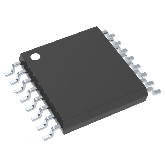
CD4027BPW

Why Choose Us?
Professional Platform
B2B & B2C purchasingDelivery at full speed
1-2 days deliveryWide variety
Original manufacturers365 days guarantee
Responsible quality
.png)


Tech Specifications
CD4027BPW Description
CD4027BPW Description
The CD4027BPW is a dual JK-type flip-flop integrated circuit (IC) from Texas Instruments, designed for a wide range of digital applications. This IC is part of the 4000B series and is housed in a 16-TSSOP surface-mount package, making it suitable for compact and high-density designs. The CD4027BPW operates on a supply voltage range of 3V to 18V, providing flexibility in power supply requirements. It features a clock frequency of up to 24 MHz, ensuring high-speed operation for demanding applications.
CD4027BPW Features
- High-Speed Operation: With a maximum clock frequency of 24 MHz, the CD4027BPW can handle fast digital signals, making it ideal for high-speed digital circuits.
- Dual JK Flip-Flops: The IC contains two independent JK flip-flops, each with one bit of storage, providing dual functionality in a single package.
- Complementary Outputs: Each flip-flop provides complementary outputs, which can be useful for driving differential signals or reducing the need for additional inverters.
- Positive Edge Triggering: The flip-flops are triggered on the positive edge of the clock signal, ensuring reliable and predictable operation.
- Low Quiescent Current: With a quiescent current of only 4 µA, the CD4027BPW is highly energy-efficient, making it suitable for battery-powered and low-power applications.
- Wide Supply Voltage Range: The ability to operate between 3V and 18V makes the CD4027BPW versatile for various power supply configurations.
- Low Propagation Delay: The maximum propagation delay of 90ns at 15V and 50pF ensures fast signal processing and minimal latency.
- ROHS3 Compliant and REACH Unaffected: The CD4027BPW meets stringent environmental standards, making it suitable for environmentally conscious designs.
- Moisture Sensitivity Level 1: The unlimited moisture sensitivity level ensures the IC is robust against environmental moisture, enhancing reliability in various operating conditions.
CD4027BPW Applications
The CD4027BPW is well-suited for a variety of applications due to its dual JK flip-flops and versatile features. Some specific use cases include:
- Digital Counters: The JK flip-flops can be configured to create synchronous counters, making the CD4027BPW ideal for applications requiring precise timing and counting.
- Frequency Dividers: The IC can be used to divide input frequencies, useful in clock generation and signal processing circuits.
- Data Storage and Latching: The flip-flops can store and latch data bits, making them suitable for memory and data handling applications.
- Sequential Logic Circuits: The CD4027BPW can be employed in designing state machines and other sequential logic circuits that require reliable and predictable operation.
- Communication Systems: The complementary outputs and high-speed operation make the IC suitable for digital communication systems where signal integrity is crucial.
Conclusion of CD4027BPW
The CD4027BPW from Texas Instruments is a robust and versatile dual JK-type flip-flop IC, offering high-speed operation, low power consumption, and a wide supply voltage range. Its complementary outputs, positive edge triggering, and low propagation delay make it an excellent choice for a variety of digital applications, including counters, frequency dividers, and sequential logic circuits. The CD4027BPW's compliance with environmental standards and its moisture sensitivity level further enhance its reliability and suitability for modern electronic designs.
FAQ
| Quantity | Unit Price | Ext. Price |
|---|---|---|
| 1+ | $0.91520 | $0.92 |
| 10+ | $0.65912 | $6.59 |
| 90+ | $0.52927 | $47.63 |
| 180+ | $0.50229 | $90.41 |
| 270+ | $0.48876 | $131.97 |
Not available to buy online? Want the lower wholesale price? Please Send RFQ to get best price, we will respond immediately


.png?x-oss-process=image/format,webp/resize,h_32)


