

Texas Instruments
CD4014BM96
Shift Registers

Not available to buy online? Want the lower wholesale price? Please Send RFQ to get best price, we will respond immediately


.png?x-oss-process=image/format,webp/resize,p_30)


CD4014BM96 Description
CD4014BM96 Description
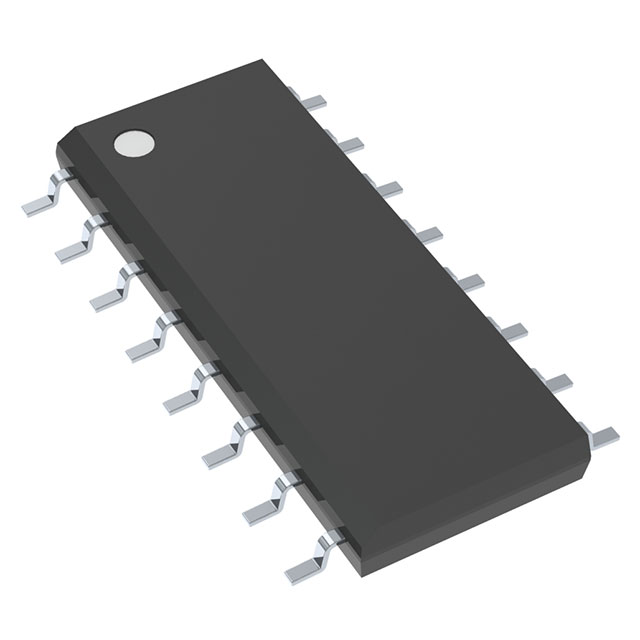
The CD4014BM96 from Texas Instruments is an 8-bit static shift register belonging to the 4000B series, designed for high-reliability digital applications. This surface-mount (SOIC-16) device operates over a wide voltage range (3V to 18V), making it versatile for both low-power and industrial systems. It supports parallel or serial-to-serial data conversion, enabling flexible data handling in sequential logic circuits. With RoHS3 compliance and REACH unaffected status, it meets stringent environmental standards while maintaining robust performance in harsh conditions.
CD4014BM96 Features
- 8-bit parallel/serial input with serial output for efficient data shifting.
- Wide supply voltage range (3V–18V), ensuring compatibility with TTL, CMOS, and mixed-voltage systems.
- Low power consumption typical of CMOS technology, ideal for battery-operated devices.
- Static operation allows data retention without clocking, reducing dynamic power loss.
- Moisture Sensitivity Level (MSL) 1 (Unlimited), suitable for extended storage and handling.
- Tape & Reel (TR) packaging for automated assembly, improving manufacturing efficiency.
CD4014BM96 Applications
- Data buffering and expansion in microcontrollers and embedded systems.
- Serial-to-parallel conversion for display drivers (e.g., LED matrices, LCDs).
- Industrial control systems requiring reliable shift registers for sensor data processing.
- Communication interfaces (e.g., UART, SPI) where synchronized data transfer is critical.
- Battery-powered devices leveraging its low-voltage operation and minimal power draw.
Conclusion of CD4014BM96
The CD4014BM96 stands out for its wide voltage tolerance, static operation, and flexible I/O modes, offering superior reliability compared to dynamic shift registers. Its industry-standard packaging and environmental compliance make it a preferred choice for high-volume production. Whether used in consumer electronics, industrial automation, or communication systems, this shift register delivers consistent performance, making it a cornerstone component for sequential logic designs.
Tech Specifications
CD4014BM96 Documents
Download datasheets and manufacturer documentation for CD4014BM96
Mult Dev Wafer Fab Site 22/Dec/2023 CD4014B,21B Types CD4014B,21B Types Mult Devices Font 21/Apr/2018 Related Parts


Shopping Guide


.png?x-oss-process=image/format,webp/resize,h_32)


©2025 ERSA Electronics Corporation.