
 German
 Japanese
 Portuguese
 Korea
Korea
 Mexico
 Dutch
Dutch


Texas Instruments
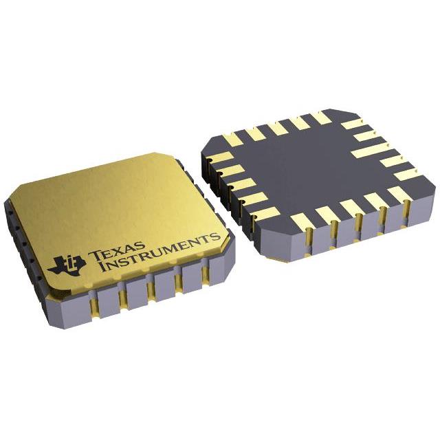
CD4016BF3A

Why Choose Us?
Professional Platform
B2B & B2C purchasingDelivery at full speed
1-2 days deliveryWide variety
Original manufacturers365 days guarantee
Responsible quality
.png)


Tech Specifications
CD4016BF3A Description
CD4016BF3A Description
The CD4016BF3A is a CMOS Quad Bilateral Switch IC, designed for a wide range of applications where signal switching is required. Manufactured by Texas Instruments, this logic IC chip belongs to the CD4016B series and is housed in a through-hole package, making it suitable for both prototyping and production environments. The CD4016BF3A features four independent circuits, each capable of operating as a 1:1 switch, providing flexibility in signal routing and control.
CD4016BF3A Features
- Quad Bilateral Switching: The CD4016BF3A offers four independent bilateral switches, each capable of handling analog or digital signals. This configuration allows for versatile signal routing and control in complex electronic systems.
- Wide Supply Voltage Range: With a supply voltage range of 3V to 18V, the CD4016BF3A can operate in a variety of power supply environments, making it suitable for both low-power and higher voltage applications.
- Dual Supply Operation: The dual supply capability ensures stable performance across different power configurations, enhancing the reliability of the device in diverse operating conditions.
- CMOS Technology: Utilizing CMOS technology, the CD4016BF3A provides low power consumption and high noise immunity, which are critical for maintaining signal integrity and reducing power usage.
- Through-Hole Mounting: The through-hole package type facilitates easy integration into printed circuit boards (PCBs) and is ideal for applications requiring robust mechanical stability.
- ROHS3 Compliant: The CD4016BF3A meets the stringent ROHS3 compliance standards, ensuring it is environmentally friendly and suitable for use in a wide range of industries.
- Active Product Status: As an active product, the CD4016BF3A is readily available and supported by Texas Instruments, providing customers with reliable supply chain and technical support.
CD4016BF3A Applications
The CD4016BF3A is ideal for applications that require precise signal switching and control. Some specific use cases include:
- Audio Signal Routing: In audio systems, the CD4016BF3A can be used to switch between different audio sources, ensuring clean and reliable signal paths.
- Data Acquisition Systems: For data acquisition systems, the ability to switch between multiple sensors or input channels is crucial. The CD4016BF3A provides a reliable solution for such applications.
- Telecommunications: In telecommunication equipment, signal switching is essential for managing multiple communication channels. The CD4016BF3A offers a robust solution for these needs.
- Medical Equipment: In medical devices, where signal integrity and reliability are paramount, the CD4016BF3A ensures precise control and switching of critical signals.
- Automotive Electronics: For automotive applications, the CD4016BF3A can be used in various systems, such as infotainment and sensor networks, where signal switching is necessary.
Conclusion of CD4016BF3A
The CD4016BF3A from Texas Instruments is a versatile and reliable CMOS Quad Bilateral Switch IC, offering four independent 1:1 switches with a wide supply voltage range of 3V to 18V. Its dual supply operation and through-hole mounting make it suitable for a variety of applications, from audio systems to medical equipment. The device's CMOS technology ensures low power consumption and high noise immunity, while its ROHS3 compliance and active product status provide environmental and supply chain advantages. The CD4016BF3A is an excellent choice for engineers and designers looking for a robust and flexible signal switching solution.
FAQ
Not available to buy online? Want the lower wholesale price? Please Send RFQ to get best price, we will respond immediately


.png?x-oss-process=image/format,webp/resize,h_32)


