
 German
 Japanese
 Portuguese
 Korea
Korea
 Mexico
 Dutch
Dutch


Texas Instruments
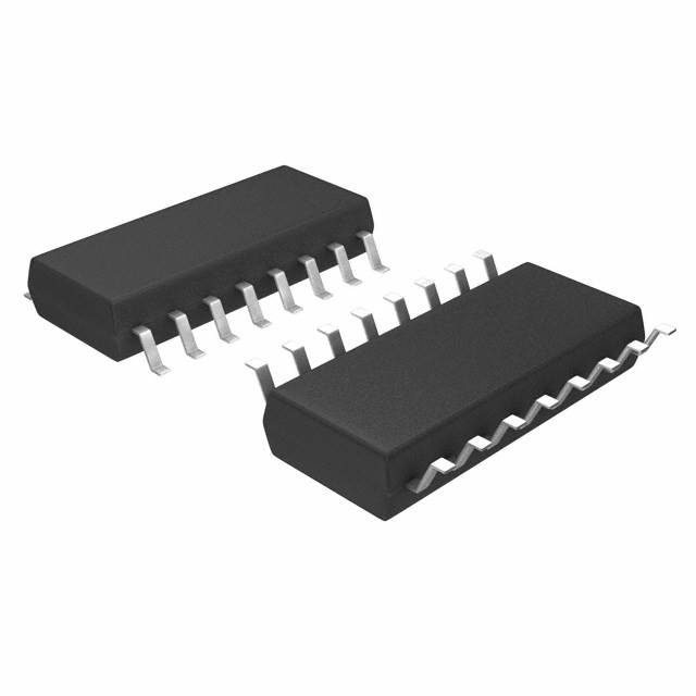
CD4049UBNSR

Why Choose Us?
Professional Platform
B2B & B2C purchasingDelivery at full speed
1-2 days deliveryWide variety
Original manufacturers365 days guarantee
Responsible quality
.png)


Tech Specifications
CD4049UBNSR Description
CD4049UBNSR Description
The CD4049UBNSR is a high-performance, 6-channel inverter integrated circuit (IC) manufactured by Texas Instruments. This IC belongs to the 4000B series and is designed for a wide range of applications in the electronics industry. The CD4049UBNSR offers excellent technical specifications, making it a popular choice for various applications.
CD4049UBNSR Features
- Logic Type: Inverter
- Max Propagation Delay: 50ns @ 15V, 50pF
- Voltage - Supply: 3V ~ 18V
- Input Logic Level - Low: 1V ~ 2.5V
- Input Logic Level - High: 4V ~ 12.5V
- Current - Quiescent (Max): 4 µA
- Current - Output High, Low: 4.3mA, 24mA
- Number of Inputs: 1
- Number of Circuits: 6
- Mounting Type: Surface Mount
- Package: Tape & Reel (TR)
- REACH Status: REACH Unaffected
- RoHS Status: ROHS3 Compliant
- Moisture Sensitivity Level (MSL): 1 (Unlimited)
The CD4049UBNSR stands out from similar models due to its low propagation delay, wide supply voltage range, and low quiescent current. These features make it ideal for power-sensitive applications and high-speed digital systems.
CD4049UBNSR Applications
The CD4049UBNSR is widely used in various applications, including:
- Digital Logic Circuits: The CD4049UBNSR's inverting functionality makes it suitable for implementing NOT gates in digital logic circuits.
- Signal Conditioning: Its ability to handle a wide range of input logic levels makes it ideal for signal conditioning applications.
- Power-Sensitive Systems: The low quiescent current of the CD4049UBNSR makes it suitable for battery-powered devices and other power-sensitive systems.
- Automotive Electronics: The wide supply voltage range and low quiescent current make the CD4049UBNSR suitable for automotive electronics applications.
Conclusion of CD4049UBNSR
In conclusion, the CD4049UBNSR is a versatile, high-performance inverter IC that offers excellent technical specifications and performance benefits. Its unique features, such as low propagation delay, wide supply voltage range, and low quiescent current, make it an ideal choice for a wide range of applications in the electronics industry. With its proven reliability and performance, the CD4049UBNSR is a trusted component in digital logic circuits, signal conditioning, power-sensitive systems, and automotive electronics.
FAQ
| Quantity | Unit Price | Ext. Price |
|---|---|---|
| 1+ | $0.57200 | $0.57 |
| 10+ | $0.40216 | $4.02 |
| 25+ | $0.36045 | $9.01 |
| 100+ | $0.31495 | $31.50 |
| 250+ | $0.29318 | $73.30 |
Not available to buy online? Want the lower wholesale price? Please Send RFQ to get best price, we will respond immediately


.png?x-oss-process=image/format,webp/resize,h_32)


