
 German
 Japanese
 Portuguese
 Korea
Korea
 Mexico
 Dutch
Dutch


Texas Instruments
CD4050BDW

Why Choose Us?
Professional Platform
B2B & B2C purchasingDelivery at full speed
1-2 days deliveryWide variety
Original manufacturers365 days guarantee
Responsible quality
.png)


Tech Specifications
CD4050BDW Description
CD4050BDW Description
The CD4050BDW is a high-performance, non-inverting buffer logic IC chip, part of the renowned 4000B series manufactured by Texas Instruments. This device is designed to provide robust and reliable signal buffering with a wide supply voltage range of 3V to 18V, making it highly versatile for various electronic applications. The CD4050BDW features six independent buffer elements, each capable of handling one bit of data, ensuring efficient signal transmission and amplification.
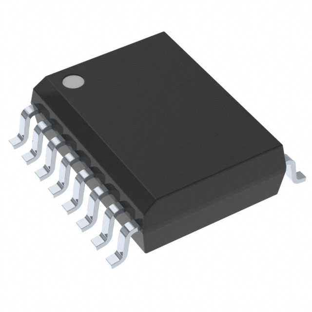
The CD4050BDW is packaged in a surface-mount 16SOIC format, which is ideal for compact and space-constrained designs. It is also housed in a tube package, facilitating easy handling and storage. This IC is compliant with REACH and ROHS3 standards, ensuring it meets environmental and safety regulations. Additionally, it has a moisture sensitivity level (MSL) of 1, which means it is not moisture-sensitive and can be stored without special packaging for an unlimited time.
CD4050BDW Features
- Wide Supply Voltage Range: The CD4050BDW operates within a supply voltage range of 3V to 18V, offering flexibility in power supply options and compatibility with a variety of electronic systems.
- High Output Current Capability: Each buffer element can source up to 8mA and sink up to 48mA, ensuring robust performance even under demanding load conditions.
- Non-Inverting Buffers: The six buffer elements provide non-inverting signal amplification, maintaining the integrity of the input signal while enhancing its strength for further transmission.
- Surface Mount Technology (SMT): The surface-mount 16SOIC package is suitable for modern, compact PCB designs, enabling high-density layouts and efficient use of space.
- Environmental Compliance: The CD4050BDW is REACH unaffected and ROHS3 compliant, making it suitable for environmentally conscious applications and ensuring regulatory compliance.
- Moisture Sensitivity Level 1: This classification means the IC can be stored and handled without moisture-sensitive precautions, simplifying logistics and reducing the risk of moisture-related damage.
CD4050BDW Applications
The CD4050BDW is ideal for a wide range of applications where signal buffering and amplification are required. Its wide voltage range and high current capability make it suitable for:
- Digital Signal Processing: Enhancing weak digital signals for reliable transmission over longer distances.
- Microcontroller Interfaces: Buffering signals between microcontrollers and peripheral devices to ensure signal integrity and reduce noise.
- Communication Systems: Amplifying signals in data transmission lines to maintain signal strength and quality.
- Power Management: Buffering control signals in power supply circuits to ensure stable operation.
- Consumer Electronics: Used in various consumer devices where compact and reliable signal buffering is necessary.
Conclusion of CD4050BDW
The CD4050BDW by Texas Instruments stands out as a versatile and reliable non-inverting buffer IC, offering a wide supply voltage range, high output current capability, and environmental compliance. Its surface-mount package and moisture sensitivity level 1 classification make it suitable for modern, compact designs and easy handling. The CD4050BDW is ideal for applications requiring robust signal buffering and amplification, making it a valuable component in digital signal processing, microcontroller interfaces, communication systems, power management, and consumer electronics.
FAQ
| Quantity | Unit Price | Ext. Price |
|---|---|---|
| 1+ | $1.00320 | $1.00 |
| 10+ | $0.72248 | $7.22 |
| 40+ | $0.62392 | $24.96 |
| 120+ | $0.56885 | $68.26 |
| 280+ | $0.53658 | $150.24 |
Not available to buy online? Want the lower wholesale price? Please Send RFQ to get best price, we will respond immediately


.png?x-oss-process=image/format,webp/resize,h_32)


