
 German
 Japanese
 Portuguese
 Korea
Korea
 Mexico
 Dutch
Dutch


Texas Instruments
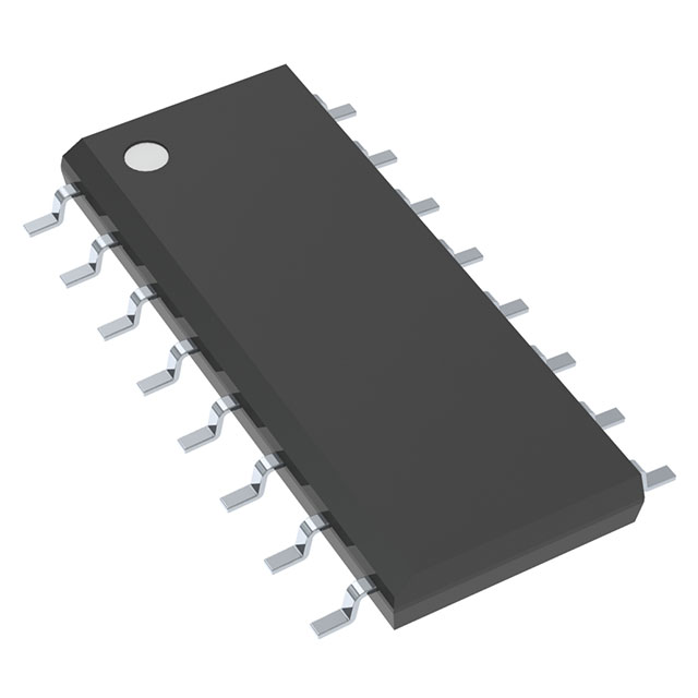
CD4052BM

Why Choose Us?
Professional Platform
B2B & B2C purchasingDelivery at full speed
1-2 days deliveryWide variety
Original manufacturers365 days guarantee
Responsible quality
.png)


Tech Specifications
CD4052BM Description
CD4052BM Description
The CD4052BM from Texas Instruments is a dual 4:1 analog multiplexer/demultiplexer IC designed for high-performance signal routing in mixed-signal applications. Housed in a 16-SOIC package, it features SP4T (Single Pole 4 Throw) switch circuits with low on-state resistance (240Ω max) and minimal leakage current (100nA max). It supports dual (±2.5V to ±9V) or single (3V to 20V) supply voltages, making it versatile for both bipolar and unipolar systems. With a -3dB bandwidth of 25MHz and low channel capacitance (0.2pF off-state, 18pF on-state), it ensures minimal signal distortion in high-frequency applications.
CD4052BM Features
- Low On-Resistance: 240Ω max ensures minimal signal attenuation.
- Wide Voltage Range: Operates at ±2.5V to ±9V (dual) or 3V to 20V (single), accommodating diverse system requirements.
- High Bandwidth: 25MHz -3dB bandwidth for high-speed signal switching.
- Low Leakage & Capacitance: 100nA max leakage and 0.2pF/18pF capacitance reduce crosstalk and power loss.
- Matched Channels: 5Ω channel-to-channel matching for consistent performance.
- Robust Packaging: 16-SOIC with MSL 1 (Unlimited) moisture sensitivity, suitable for industrial environments.
- Compliance: RoHS3 and REACH Unaffected, meeting global environmental standards.
CD4052BM Applications
- Audio/Video Routing: Ideal for signal selection in AV switches due to low distortion.
- Data Acquisition Systems: High accuracy in multiplexing sensor signals.
- Test & Measurement Equipment: Reliable switching for precision instruments.
- Communication Systems: Low crosstalk benefits RF and baseband signal routing.
- Industrial Control: Robust performance in harsh environments.
Conclusion of CD4052BM
The CD4052BM excels in low-noise, high-speed signal switching with its low on-resistance, wide voltage range, and superior channel matching. Its dual-supply capability and 25MHz bandwidth make it a standout choice for mixed-signal, audio, and measurement systems. While marked as Last Time Buy, its REACH/RoHS compliance and industrial-grade reliability ensure long-term suitability for critical designs. Engineers should consider this IC for precision analog routing where performance and stability are paramount.
FAQ
| Quantity | Unit Price | Ext. Price |
|---|---|---|
| 1+ | $1.02080 | $1.02 |
| 10+ | $0.73568 | $7.36 |
| 40+ | $0.63580 | $25.43 |
Not available to buy online? Want the lower wholesale price? Please Send RFQ to get best price, we will respond immediately


.png?x-oss-process=image/format,webp/resize,h_32)


