
 German
 Japanese
 Portuguese
 Korea
Korea
 Mexico
 Dutch
Dutch


Texas Instruments
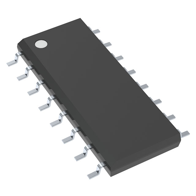
CD4052BM96

Why Choose Us?
Professional Platform
B2B & B2C purchasingDelivery at full speed
1-2 days deliveryWide variety
Original manufacturers365 days guarantee
Responsible quality
.png)


Tech Specifications
CD4052BM96 Description
CD4052BM96 is a dual analog multiplexer/demultiplexer device manufactured by Texas Instruments. It is a member of the 4050 family of analog multiplexers and demultiplexers, which are widely used in various electronic applications for routing signals between multiple input channels and a single output channel, or vice versa.
Description:
The CD4052BM96 is a monolithic integrated circuit that contains two independent analog multiplexers/demultiplexers. Each multiplexer/demultiplexer has 8 input channels and 1 output channel. The device can be used as a multiplexer to select one of the eight input signals to be routed to the output, or as a demultiplexer to distribute a single input signal to one of the eight output channels.
Features:
- Dual 8-channel multiplexer/demultiplexer in a single package
- Analog signal handling capability
- Low input offset voltage and low input bias current
- Wide supply voltage range (3V to 15V)
- High channel isolation (up to 70dB)
- Low on-resistance (typically 40 ohms)
- TTL-compatible control inputs
- Available in a 16-pin dual-in-line package (DIP)
Applications:
- Audio signal routing in audio mixing consoles
- Signal routing in medical equipment and instrumentation
- Data acquisition systems and multiplexing
- Test and measurement equipment
- Telecommunication systems
- Industrial control systems
- Signal distribution in video and audio matrix switching applications
- Analog signal switching in various signal processing applications
The CD4052BM96 is a versatile and reliable component for signal routing and distribution in a wide range of electronic systems. Its dual-channel architecture allows for efficient use of space on a printed circuit board and simplifies system design by reducing the number of components required.
FAQ
| Quantity | Unit Price | Ext. Price |
|---|---|---|
| 1+ | $0.38720 | $0.39 |
| 10+ | $0.27280 | $2.73 |
| 25+ | $0.24323 | $6.08 |
| 100+ | $0.21094 | $21.09 |
| 250+ | $0.19550 | $48.88 |
Not available to buy online? Want the lower wholesale price? Please Send RFQ to get best price, we will respond immediately


.png?x-oss-process=image/format,webp/resize,h_32)


