
Texas Instruments
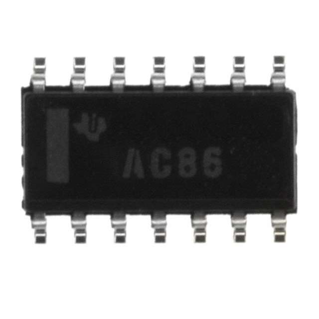
SN74HC4066DBR
Analog Switches, Multiplexers, Demultiplexers


.png?x-oss-process=image/format,webp/resize,p_30)


SN74HC4066DBR Description
The Texas Instruments SN74HC4066DBR is a high-performance, 14-channel multiplexer/demultiplexer integrated circuit (IC) that is commonly used in digital signal processing and communication systems. It is designed to efficiently route signals between multiple input lines and a single output line, or vice versa, depending on the control signals applied.
Description:
The SN74HC4066DBR is a member of the 74HC series of CMOS logic devices, which are known for their high-speed performance and low power consumption. The device is available in a compact, thermally enhanced, and leadless (DFN) package, making it suitable for use in a wide range of applications, including portable and battery-powered devices.
Features:
- 14 input lines, 4 output lines: The SN74HC4066DBR can handle up to 14 input lines and provide 4 output lines, allowing for efficient signal routing and management.
- Low power consumption: The device is designed to operate with low power consumption, making it suitable for energy-sensitive applications.
- High-speed performance: The SN74HC4066DBR offers high-speed performance, with a propagation delay of typically 3.6 ns (typical) and a maximum operating frequency of 100 MHz.
- Wide operating voltage range: The device can operate over a wide voltage range of 2.0V to 6.0V, making it suitable for various power supply requirements.
- Low on-resistance: The on-resistance of the multiplexer is typically 100 ohms, ensuring low signal loss and high signal integrity.
- Active-low enable input: The enable input (E) allows the device to be put in a high-impedance state, effectively disconnecting the input lines from the output lines.
Applications:
- Digital signal processing: The SN74HC4066DBR can be used in digital signal processing applications to route and manage multiple input signals.
- Communication systems: The device can be used in communication systems for signal routing and multiplexing/demultiplexing tasks.
- Audio and video applications: The SN74HC4066DBR can be used in audio and video applications for signal routing and channel selection.
- Medical equipment: The device can be used in medical equipment for signal routing and management, particularly in portable and battery-powered devices.
- Industrial control systems: The SN74HC4066DBR can be used in industrial control systems for signal routing and multiplexing/demultiplexing tasks.
- Test and measurement equipment: The device can be used in test and measurement equipment for signal routing and channel selection.
In summary, the Texas Instruments SN74HC4066DBR is a versatile and high-performance multiplexer/demultiplexer IC that offers a range of features, including low power consumption, high-speed performance, and a wide operating voltage range. It is suitable for a variety of applications, including digital signal processing, communication systems, audio and video applications, medical equipment, industrial control systems, and test and measurement equipment.
Tech Specifications
SN74HC4066DBR Documents
Download datasheets and manufacturer documentation for SN74HC4066DBR
 SN74HC4066
  Replacement Update 14/Jun/2023 Mult Dev EOL 21/Jun/2023
  SN74HC4066
 Shopping Guide


.png?x-oss-process=image/format,webp/resize,h_32)


