

Texas Instruments
TMUX1112PWR
Analog Switches, Multiplexers, Demultiplexers

Not available to buy online? Want the lower wholesale price? Please Send RFQ to get best price, we will respond immediately


.png?x-oss-process=image/format,webp/resize,p_30)


TMUX1112PWR Description
TMUX1112PWR Description
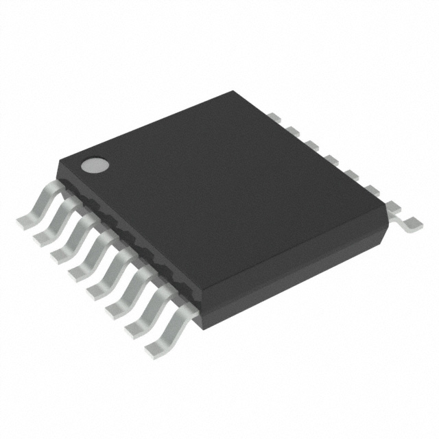
The TMUX1112PWR from Texas Instruments is a high-performance, quad-channel SPST (Single-Pole Single-Throw) analog switch designed for precision signal routing in low-voltage applications. Packaged in a 16-pin TSSOP and available in Tape & Reel (TR), this device operates over a wide supply voltage range of 1.08V to 5.5V, making it versatile for both portable and industrial systems. With an ultra-low leakage current of 80pA (max) and minimal on-state resistance (4Ω max), it ensures minimal signal distortion and power loss. The device is RoHS3 compliant and REACH unaffected, meeting stringent environmental standards.
TMUX1112PWR Features
- Low On-Resistance: 4Ω (max) ensures minimal voltage drop and high signal fidelity.
- Ultra-Low Leakage: 80pA (max) reduces power waste in battery-operated devices.
- Wide Bandwidth: 300MHz -3dB bandwidth supports high-speed signal switching.
- Low Channel Capacitance: 7pF (CS(off)) / 10pF (CD(off)) minimizes crosstalk and signal distortion.
- Excellent Matching: 130mΩ ΔRon ensures consistent performance across channels.
- Robust Packaging: 16-TSSOP with MSL1 (Unlimited) rating for reliable surface-mount assembly.
- Broad Voltage Range: 1.08V–5.5V compatibility for mixed-voltage systems.
TMUX1112PWR Applications
- Portable Electronics: Ideal for battery-powered devices due to low leakage and wide voltage range.
- Test & Measurement Systems: High bandwidth and low distortion suit signal multiplexing in oscilloscopes and data acquisition.
- Industrial Automation: Reliable switching for sensor interfaces and PLCs.
- Medical Devices: Precision signal routing in patient monitoring and diagnostic equipment.
- Communications: Low capacitance and high bandwidth benefit RF and baseband signal switching.
Conclusion of TMUX1112PWR
The TMUX1112PWR stands out for its low on-resistance, ultra-low leakage, and high bandwidth, making it a superior choice for precision analog switching. Its wide supply range and robust packaging cater to diverse applications, from wearables to industrial systems. Compared to similar models, its exceptional channel matching and low capacitance ensure reliable performance in high-frequency and low-power scenarios. Engineers seeking a high-performance, space-efficient analog switch will find this device an optimal solution.
Tech Specifications
TMUX1112PWR Documents
Download datasheets and manufacturer documentation for TMUX1112PWR
Product Change Notification (PDF) TMUX1112PWR Symbol & Footprint by SnapMagic Related Parts


Shopping Guide


.png?x-oss-process=image/format,webp/resize,h_32)


©2025 ERSA Electronics Corporation.