
Texas Instruments
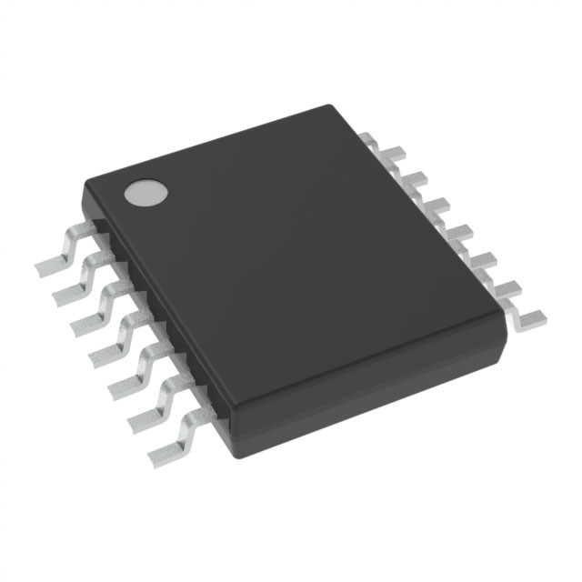
CD4093BPWR
Gates and Inverters


.png?x-oss-process=image/format,webp/resize,p_30)


CD4093BPWR Description
The Texas Instruments CD4093BPWR is a high-performance, quad 2-input multiplexer (MUX) (IC) designed for a wide range of applications in digital signal processing and communication systems. This IC is part of the 4000 series of CMOS devices, which are known for their low power consumption and high noise immunity.
Description:
The CD4093BPWR is a monolithic integrated circuit that contains four independent 2-input multiplexers. Each multiplexer has two data inputs (A and B), two select inputs (S and S'), and one output (Y). The IC is designed to handle both positive and negative logic levels, making it suitable for various digital systems.
Features:
- Quad 2-input multiplexers: The IC contains four independent multiplexers, providing a total of eight data inputs and four outputs.
- Positive and negative logic compatible: The CD4093BPWR can handle both types of logic levels, making it versatile for different applications.
- Low power consumption: As a CMOS device, the CD4093BPWR offers low power consumption, which is ideal for battery-powered or energy-efficient applications.
- High noise immunity: The IC is designed to operate with high noise immunity, ensuring reliable performance in noisy environments.
- Wide supply voltage range: The CD4093BPWR can operate with a supply voltage range of 3V to 15V, making it suitable for various power supply configurations.
- Available in a 16-pin package: The IC is available in a standard 16-pin package, making it easy to integrate into existing designs.
Applications:
- Digital signal processing: The CD4093BPWR can be used in digital signal processing applications, such as audio processing, filtering, and data conversion.
- Communication systems: The IC can be used in communication systems for routing digital signals, such as in multiplexing/demultiplexing applications.
- Data routing and switching: The CD4093BPWR can be used in data routing and switching applications, where multiple data streams need to be selectively routed to different destinations.
- Logic level conversion: The IC can be used to convert between positive and negative logic levels in digital systems.
- Memory address decoding: The CD4093BPWR can be used in memory address decoding applications, where multiple memory addresses need to be selectively accessed.
- Control systems: The IC can be used in control systems for routing control signals based on input conditions.
In summary, the Texas Instruments CD4093BPWR is a versatile and high-performance quad 2-input multiplexer IC that offers a range of features, including compatibility with both positive and negative logic levels, low power consumption, and high noise immunity. It is suitable for various applications in digital signal processing, communication systems, data routing, and control systems.
Tech Specifications
CD4093BPWR Documents
Download datasheets and manufacturer documentation for CD4093BPWR
 CD4093B Types
  Symbolization Update 28/Nov/2022
  CD4093B Types
  Design 22/Feb/2022
 Shopping Guide


.png?x-oss-process=image/format,webp/resize,h_32)


