
 German
 Japanese
 Portuguese
 Korea
Korea
 Mexico
 Dutch
Dutch


Texas Instruments
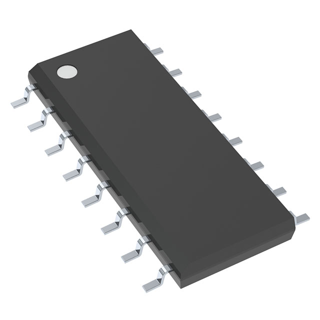
CD4099BM

Why Choose Us?
Professional Platform
B2B & B2C purchasingDelivery at full speed
1-2 days deliveryWide variety
Original manufacturers365 days guarantee
Responsible quality
.png)


Tech Specifications
CD4099BM Description
CD4099BM Description
The CD4099BM from Texas Instruments is a high-performance 8-bit addressable latch designed for surface-mount applications in the 4000B series. Operating within a wide voltage range of 3V to 18V, this latch is ideal for low-to-medium power digital systems. It features standard output type with symmetrical 6.8mA output current (high and low), ensuring reliable signal integrity. With a propagation delay of 50ns, it balances speed and power efficiency, making it suitable for timing-critical applications. Packaged in a 16-SOIC tube, the CD4099BM is ROHS3 compliant and REACH unaffected, meeting stringent environmental standards.
CD4099BM Features
- 8-bit addressable latch with 1:8 circuit configuration, enabling precise data control.
- Wide supply voltage range (3V–18V), supporting compatibility with TTL and CMOS logic levels.
- High output drive capability (6.8mA sink/source) for robust signal transmission.
- Low propagation delay (50ns), ensuring efficient timing in sequential logic circuits.
- Surface-mount (SOIC-16) packaging, optimized for compact PCB designs.
- Last Time Buy status, indicating limited availability for legacy system support.
- Moisture Sensitivity Level (MSL) 1, suitable for extended storage and handling.
CD4099BM Applications
The CD4099BM excels in digital systems requiring latched data storage, such as:
- Memory address decoding in microcontrollers and FPGAs.
- Data routing and multiplexing in industrial control systems.
- LED matrix driving for display applications.
- Signal gating and buffering in communication interfaces.
Its wide voltage tolerance makes it adaptable for battery-powered devices, while its high noise immunity ensures reliability in electrically noisy environments.
Conclusion of CD4099BM
The CD4099BM is a versatile, high-reliability latch ideal for legacy and modern digital designs. Its balanced performance, robust drive capability, and compliance with environmental standards make it a preferred choice for engineers needing stable data retention in space-constrained applications. While marked as Last Time Buy, it remains a dependable solution for systems requiring long-term support.
FAQ
| Quantity | Unit Price | Ext. Price |
|---|---|---|
| 1+ | $2.02972 | $2.03 |
| 10+ | $1.98343 | $19.83 |
| 30+ | $1.95257 | $58.58 |
Not available to buy online? Want the lower wholesale price? Please Send RFQ to get best price, we will respond immediately


.png?x-oss-process=image/format,webp/resize,h_32)


