
 German
 Japanese
 Portuguese
 Korea
Korea
 Mexico
 Dutch
Dutch


Texas Instruments
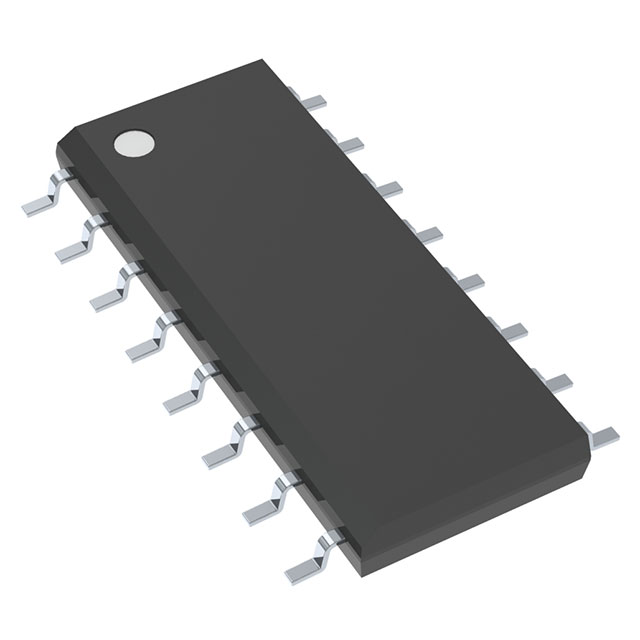
CD74HC4051M96

Why Choose Us?
Professional Platform
B2B & B2C purchasingDelivery at full speed
1-2 days deliveryWide variety
Original manufacturers365 days guarantee
Responsible quality
.png)


Tech Specifications
CD74HC4051M96 Description
The Texas Instruments CD74HC4051M96 is a high-performance integrated circuit (IC) that belongs to the family of analog multiplexers and switches. It is a 16-channel, single-pole, 16-throw analog switch that provides excellent signal routing capabilities in various applications. Here's a detailed description, features, and applications of the CD74HC4051M96:
Description:
The CD74HC4051M96 is a CMOS device designed to operate with a wide range of input signals, including low-voltage and high-impedance sources. It features 16 analog input channels that can be connected to a single output channel through a selection mechanism. The device is available in a 48-pin TSSOP (Thin Shrink Small Outline Package) package.
Features:
- 16 analog input channels.
- Single-pole, 16-throw (SP16T) configuration.
- 3-state outputs for low output impedance.
- High channel-to-channel isolation (typically 70 dB).
- Low on-resistance (typically 35 ohms).
- Wide operating voltage range (2.0V to 6.0V).
- Fast switching speed (typically 35 ns propagation delay).
- Low power consumption (typically 3 mA per channel).
- Compatible with TTL and CMOS logic levels.
- Available in a 48-pin TSSOP package.
Applications:
- Audio mixing and routing in professional audio equipment.
- Signal routing in medical equipment, such as patient monitoring systems.
- Data acquisition systems and multiplexers in industrial control applications.
- Test and measurement equipment, where signal routing and switching are required.
- Video signal routing in surveillance systems and video processing equipment.
- RF signal routing in communication systems and wireless applications.
- General-purpose signal routing and switching in various electronic systems.
The CD74HC4051M96 is a versatile and reliable analog switch that can be used in a wide range of applications where signal routing and switching are required. Its high performance, low power consumption, and compatibility with various input signal types make it a popular choice for designers working on complex electronic systems.
FAQ
| Quantity | Unit Price | Ext. Price |
|---|---|---|
| 10+ | $0.30000 | $3.00 |
| 30+ | $0.26057 | $7.82 |
| 100+ | $0.22628 | $22.63 |
| 500+ | $0.21600 | $108.00 |
| 1000+ | $0.20915 | $209.15 |
Not available to buy online? Want the lower wholesale price? Please Send RFQ to get best price, we will respond immediately


.png?x-oss-process=image/format,webp/resize,h_32)


