
 German
 Japanese
 Portuguese
 Korea
Korea
 Mexico
 Dutch
Dutch


Texas Instruments
CDC337DWR

Why Choose Us?
Professional Platform
B2B & B2C purchasingDelivery at full speed
1-2 days deliveryWide variety
Original manufacturers365 days guarantee
Responsible quality
.png)


Tech Specifications
CDC337DWR Description
CDC337DWR Description
The CDC337DWR is a fanout buffer (distribution) IC designed by Texas Instruments, offering a 1:8 input-to-output ratio. This device is specifically designed for clock buffering applications, providing high performance and reliability. It features a TTL input and CMOS output, ensuring compatibility with a wide range of digital systems. The CDC337DWR operates within a supply voltage range of 4.75V to 5.25V and supports a maximum frequency of 80 MHz, making it suitable for high-speed clock distribution tasks.
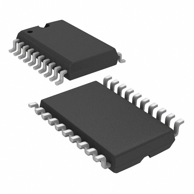
The CDC337DWR is packaged in a 20-pin SOIC format and is available in a surface-mount configuration, ideal for compact and space-efficient designs. It is categorized under Clock Buffers and Drivers ICs, and is part of the CDC337 base product family. This IC is REACH unaffected and RoHS3 compliant, ensuring it meets the latest environmental and regulatory standards. The device is moisture sensitivity level 1 (unlimited), making it suitable for a wide range of manufacturing environments.
CDC337DWR Features
- High Fanout Capability: The 1:8 input-to-output ratio allows for efficient distribution of clock signals to multiple destinations, reducing the need for additional buffering components.
- Wide Operating Voltage: Range The 4.75V to 5.25V supply voltage range ensures compatibility with various power supply configurations, enhancing its versatility.
- High-Speed Performance: With a maximum operating frequency of 80 MHz, the CDC337DWR is well-suited for high-speed clock distribution applications, ensuring minimal signal degradation.
- TTL Input and CMOS Output: This combination provides compatibility with a wide range of digital systems, making it a flexible choice for various applications.
- Surface-Mount Packaging: The 20-pin SOIC package and surface-mount configuration allow for compact and space-efficient designs, ideal for modern electronics.
- Environmental Compliance: The REACH unaffected and RoHS3 compliant status ensures that the CDC337DWR meets the latest environmental and regulatory standards.
- Moisture Sensitivity Level 1: The unlimited moisture sensitivity level makes the device suitable for a wide range of manufacturing environments, reducing the risk of damage during production.
CDC337DWR Applications
The CDC337DWR is ideal for a variety of applications requiring high-speed clock distribution and buffering. Some specific use cases include:
- Telecommunications: High-speed clock distribution in communication systems, ensuring precise timing for data transmission.
-Computer Systems: Distributing clock signals in servers and high-performance computing systems, maintaining synchronization across multiple components. - Industrial Control Systems: Providing reliable clock signals in industrial automation and control systems, ensuring accurate timing for critical operations.
- Consumer Electronics: Used in devices such as routers, modems, and set-top boxes for efficient clock signal distribution.
Conclusion of CDC337DWR
The CDC337DWR, designed by Texas Instruments, is a robust and versatile fanout buffer IC that offers high performance and reliability. Its 1:8 input-to-output ratio, wide operating voltage range, and high-speed capabilities make it an ideal choice for a variety of applications requiring efficient clock distribution. The device's surface-mount configuration and compact packaging ensure it can be easily integrated into modern electronics designs. With its environmental compliance and moisture sensitivity level 1 rating, the CDC337DWR is well-suited for a wide range of manufacturing environments. Despite its obsolete status, the CDC337DWR remains a valuable component for applications requiring high-speed clock distribution and buffering.
FAQ
Not available to buy online? Want the lower wholesale price? Please Send RFQ to get best price, we will respond immediately


.png?x-oss-process=image/format,webp/resize,h_32)


