
 German
 Japanese
 Portuguese
 Korea
Korea
 Mexico
 Dutch
Dutch


Texas Instruments
CDCDB400RHBT

Why Choose Us?
Professional Platform
B2B & B2C purchasingDelivery at full speed
1-2 days deliveryWide variety
Original manufacturers365 days guarantee
Responsible quality
.png)


Tech Specifications
CDCDB400RHBT Description
CDCDB400RHBT Description
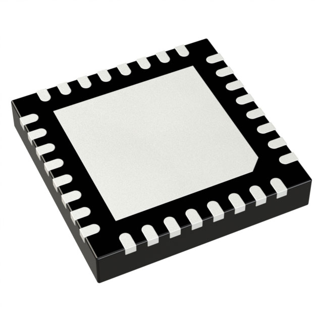
The CDCDB400RHBT is a high-performance clock buffer designed by Texas Instruments, offering a 1:4 input-to-output ratio. This device is specifically engineered to handle high-frequency clock signals, making it suitable for demanding applications requiring precise timing and signal distribution. The CDCDB400RHBT supports differential input and output, ensuring robust signal integrity and minimal jitter. It operates within a supply voltage range of 3V to 3.6V and is housed in a 32-pin VQFN package, which is ideal for-mount surface applications. With a maximum operating frequency of 250 MHz, this clock buffer is well-suited for high-speed digital systems. The device is categorized under Clock/Timing ICs and is currently in an active product status, ensuring availability for new designs.
CDCDB400RHBT Features
- High-Frequency Performance: The CDCDB400RHBT supports a maximum frequency of 250 MHz, making it suitable for high-speed applications where precise timing is.
critical- Differential Signaling: Both input and output are differential, which enhances signal integrity by reducing electromagnetic interference and improving noise immunity. - Flexible Supply Voltage: The device operates within a 3V to 3.6V supply voltage range, providing flexibility in power supply design.
- Surface-Mount Compatibility: The 32-pin VQFN package is ideal for surface-mount technology (SMT), enabling compact and reliable PCB.
designs- Single Circuit Design: With a single circuit, the CDCDB400RHBT simplifies design integration and reduces complexity. - Moisture Sensitivity Level (MSL) 1: The device is rated for unlimited exposure to moisture, making it suitable for a wide range of environmental conditions.
- RoHS Compliance: The CDCDB400RHBT is not subject to RoHS restrictions, ensuring compliance with environmental regulations.
CDCDB400RHBT Applications
The CDCDB400RHBT is ideal for a variety of applications where high-frequency clock distribution and signal integrity are paramount. Some specific use cases include-:
High-Speed Digital Systems: Ideal for applications such as high-speed networking equipment, where precise clock distribution is essential for maintaining data integrity.
- Telecommunications: Suitable for telecom infrastructure, where reliable clock buffering is necessary for synchronization across multiple components.
- Data Centers: Beneficial in data center environments, where high-frequency clock signals need to be distributed with minimal jitter.
- Industrial Automation: Applicable in industrial control systems, where robust and reliable clock distribution is required for real-time processing and control.
- Consumer Electronics: Can be used in high-performance consumer devices, such as gaming consoles and high-definition video processing units, where precise timing is crucial.
Conclusion of CDCDB400RHBT
The CDCDB400RHBT from Texas Instruments stands out as a reliable and high-performance clock buffer, offering a 1:4 input-to-output ratio with differential signaling capabilities. Its ability to operate at frequencies up to 250 MHz makes it a versatile component for a wide range of high-speed applications. The device's surface-mount compatibility and moisture resistance further enhance its suitability for various industrial and consumer electronics applications The. CDCDB400RHBT's robust design and high-frequency performance make it an excellent choice for engineers seeking a reliable clock buffer solution.
FAQ
| Quantity | Unit Price | Ext. Price |
|---|---|---|
| 1+ | $3.59920 | $3.60 |
| 10+ | $2.72448 | $27.24 |
| 25+ | $2.50554 | $62.64 |
| 100+ | $2.26459 | $226.46 |
| 250+ | $2.14966 | $537.41 |
Not available to buy online? Want the lower wholesale price? Please Send RFQ to get best price, we will respond immediately


.png?x-oss-process=image/format,webp/resize,h_32)


