

Texas Instruments
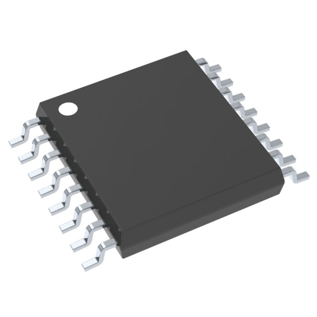
CDCE925PWR
Clock Generators & Support Products

Not available to buy online? Want the lower wholesale price? Please Send RFQ to get best price, we will respond immediately


- 1+
- $4.87030
- $4.87
- 10+
- $4.20293
- $42.03
- 30+
- $3.80714
- $114.21

.png?x-oss-process=image/format,webp/resize,p_30)


CDCE925PWR Description
The Texas Instruments CDCE925PWR is a high-performance, low-power, precision voltage reference IC that provides excellent stability and accuracy over a wide range of operating conditions. It is designed to offer a precise and stable voltage reference for various applications, including industrial, medical, and consumer electronics.
Description:
The CDCE925PWR is a fixed voltage reference IC that operates from a supply voltage range of 2.5V to 5.5V. It has an output voltage of 2.5V and is available in a small, 6-pin SC70 package. The device features a low temperature coefficient of 5 ppm/°C and a low initial accuracy of ±0.05%, making it suitable for precision applications.
Features:
- Low Power Consumption: The CDCE925PWR consumes only 10 μA of supply current, making it ideal for battery-powered applications.
- High Precision: The device offers a low temperature coefficient of 5 ppm/°C and an initial accuracy of ±0.05%, ensuring stable and accurate voltage references over a wide temperature range.
- Wide Supply Voltage Range: The CDCE925PWR can operate from a supply voltage range of 2.5V to 5.5V, making it suitable for various power supply configurations.
- Small Package: The IC is available in a compact 6-pin SC70 package, which is ideal for space-constrained applications.
- Low Drift: The device has a low drift over time, ensuring long-term stability and reliability.
- Low Output Noise: The CDCE925PWR has a low output noise of 1.5 μVrms, making it suitable for applications requiring low-noise voltage references.
Applications:
- Data Acquisition Systems: The CDCE925PWR can be used as a stable voltage reference for precision data acquisition systems, ensuring accurate and reliable measurements.
- Battery-Powered Devices: The low power consumption of the device makes it suitable for battery-powered applications, such as portable medical devices and consumer electronics.
- Industrial Control Systems: The high precision and stability of the CDCE925PWR make it ideal for use in industrial control systems, where accurate voltage references are critical for reliable operation.
- Sensor Interfaces: The device can be used as a stable voltage reference for sensor interfaces, providing accurate and stable measurements in various applications, such as temperature, pressure, and humidity sensing.
- Power Management Systems: The CDCE925PWR can be used in power management systems to provide a stable voltage reference for voltage monitoring and regulation.
In summary, the Texas Instruments CDCE925PWR is a high-performance, low-power, precision voltage reference IC that offers excellent stability and accuracy over a wide range of operating conditions. Its features, such as low power consumption, high precision, and low drift, make it suitable for a variety of applications, including data acquisition systems, battery-powered devices, industrial control systems, sensor interfaces, and power management systems.
Tech Specifications
CDCE925PWR Documents
Download datasheets and manufacturer documentation for CDCE925PWR
CDCE925, CDCEL925 CDCE925, CDCEL925 Design 22/Feb/2022 Related Parts


Shopping Guide


.png?x-oss-process=image/format,webp/resize,h_32)


©2025 ERSA Electronics Corporation.