
 German
 Japanese
 Portuguese
 Korea
Korea
 Mexico
 Dutch
Dutch


Texas Instruments
CDCLVC1106PW

Why Choose Us?
Professional Platform
B2B & B2C purchasingDelivery at full speed
1-2 days deliveryWide variety
Original manufacturers365 days guarantee
Responsible quality
.png)


Tech Specifications
CDCLVC1106PW Description
CDCLVC1106PW Description
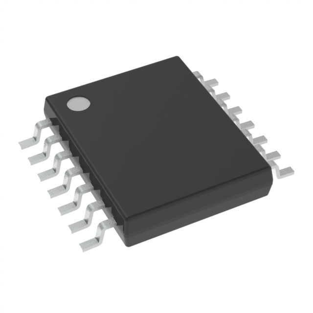
The CDCLVC1106PW from Texas Instruments is a high-performance 1:6 LVCMOS fanout buffer designed for clock distribution in demanding electronic systems. Operating within a 2.3V to 3.6V supply range, this surface-mount IC delivers robust signal integrity with a maximum frequency of 250 MHz, making it ideal for synchronizing multiple clock domains. Housed in a 14-pin TSSOP package, it features a single-input, six-output architecture with non-differential LVCMOS interfaces, ensuring compatibility with a wide range of digital systems. Its RoHS3 compliance and REACH-unaffected status further enhance its suitability for environmentally conscious designs.
CDCLVC1106PW Features
- 1:6 Clock Distribution: Provides precise signal replication across six outputs from a single LVCMOS input.
- Wide Voltage Range (2.3V–3.6V): Supports flexible integration into mixed-voltage systems.
- High-Speed Operation (250 MHz): Ensures low-jitter performance for timing-critical applications.
- Non-Differential I/O: Simplifies design by eliminating the need for differential signaling components.
- Robust Packaging: 14-pin TSSOP (Tube) with MSL 1 (Unlimited) rating for easy handling and assembly.
- Low Power Consumption: Optimized for energy-efficient designs without sacrificing performance.
CDCLVC1106PW Applications
The CDCLVC1106PW excels in applications requiring high-fidelity clock distribution, such as:
- Telecommunications Equipment: Synchronizing data converters, FPGAs, and processors in base stations.
- Networking Hardware: Clock tree management in routers, switches, and servers.
- Industrial Automation: Timing control for PLCs, motor drives, and sensors.
- Consumer Electronics: Low-jitter clocking for high-resolution displays and audio/video interfaces.
Its LVCMOS compatibility and 250 MHz capability make it particularly valuable in systems where signal integrity and low skew are critical.
Conclusion of CDCLVC1106PW
The CDCLVC1106PW stands out as a reliable, high-speed fanout buffer for LVCMOS clock distribution, offering a balance of performance, flexibility, and ease of integration. Its wide supply range, low-jitter outputs, and industry-standard compliance make it a preferred choice for engineers designing high-speed digital systems. Whether in telecom, networking, or industrial applications, this IC ensures precise timing synchronization while minimizing design complexity.
FAQ
| Quantity | Unit Price | Ext. Price |
|---|---|---|
| 1+ | $4.55840 | $4.56 |
| 10+ | $3.47952 | $34.80 |
| 90+ | $2.93089 | $263.78 |
| 180+ | $2.81703 | $507.07 |
| 270+ | $2.76004 | $745.21 |
Not available to buy online? Want the lower wholesale price? Please Send RFQ to get best price, we will respond immediately


.png?x-oss-process=image/format,webp/resize,h_32)


