

Texas Instruments
CDCLVC1103PW
Clock Buffers, Drivers ICs

Not available to buy online? Want the lower wholesale price? Please Send RFQ to get best price, we will respond immediately


.png?x-oss-process=image/format,webp/resize,p_30)


CDCLVC1103PW Description
CDCLVC1103PW Description
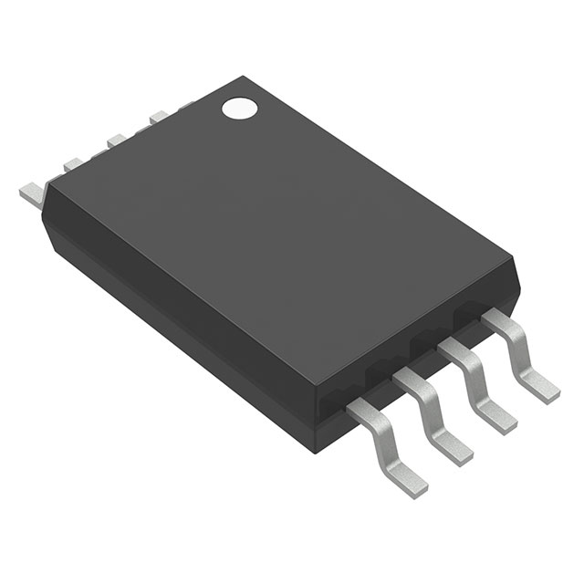
The CDCLVC1103PW from Texas Instruments is a high-performance 1:3 LVCMOS fanout buffer designed for precise clock distribution in demanding electronic systems. Operating within a 2.3V to 3.6V supply range, this surface-mount IC delivers robust signal integrity with a maximum frequency of 250 MHz, making it ideal for applications requiring low-jitter clock propagation. Its single-input, triple-output architecture ensures minimal skew and phase distortion, critical for synchronizing high-speed digital circuits. Packaged in an 8-pin TSSOP tube format, the device is RoHS3 compliant and rated for unlimited moisture sensitivity (MSL 1), ensuring reliability in industrial and commercial environments.
CDCLVC1103PW Features
- 1:3 Clock Distribution: Provides three identical LVCMOS outputs from a single LVCMOS input, reducing board space and BOM complexity.
- Wide Voltage Range (2.3V–3.6V): Compatible with mixed-voltage systems and low-power designs.
- High-Speed Operation: Supports frequencies up to 250 MHz with minimal additive jitter.
- Low Skew & Phase Error: Ensures precise timing alignment across outputs.
- Industrial Robustness: REACH unaffected, EAR99 (export-friendly), and RoHS3 compliant.
- Surface-Mount TSSOP Package: Compact footprint for space-constrained PCBs.
CDCLVC1103PW Applications
The CDCLVC1103PW excels in systems requiring low-noise clock distribution, such as:
- FPGA/ASIC Timing: Synchronizes multiple clock domains in programmable logic designs.
- Networking Equipment: Ensures stable clocking for switches, routers, and PHY interfaces.
- Test & Measurement: Provides clean clock signals for high-precision instruments.
- Consumer Electronics: Used in HDTVs, set-top boxes, and audio/video processors.
- Industrial Automation: Reliable timing for PLCs, motor controllers, and sensors.
Conclusion of CDCLVC1103PW
The CDCLVC1103PW stands out for its simplicity, performance, and reliability in clock distribution tasks. Its low-jitter outputs, wide voltage range, and industrial-grade robustness make it a superior choice over generic buffers. Whether for high-speed digital designs or noise-sensitive applications, this IC ensures consistent signal fidelity while simplifying system architecture. Engineers can leverage its TSSOP packaging and compliance certifications to streamline designs without compromising on timing accuracy.
Tech Specifications
CDCLVC1103PW Documents
Download datasheets and manufacturer documentation for CDCLVC1103PW
CDCLVC11xx CDCLVC11xx Copper Bond Wire Revision A 04/Dec/2013 Design 22/Feb/2022 Related Parts


Shopping Guide


.png?x-oss-process=image/format,webp/resize,h_32)


©2025 ERSA Electronics Corporation.