
 German
 Japanese
 Portuguese
 Korea
Korea
 Mexico
 Dutch
Dutch


Texas Instruments
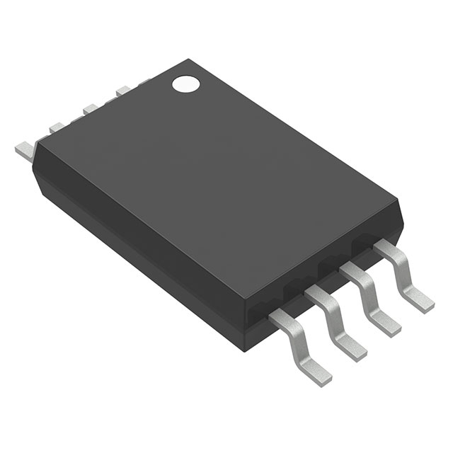
CDCS503PWR

Why Choose Us?
Professional Platform
B2B & B2C purchasingDelivery at full speed
1-2 days deliveryWide variety
Original manufacturers365 days guarantee
Responsible quality
.png)


Tech Specifications
CDCS503PWR Description
The Texas Instruments CDCS503PWR is a high-performance, low-power, mixed-signal device that combines a digital signal processor (DSP) with a microcontroller (MCU) in a single chip. It is designed for use in a wide range of applications, including industrial control, medical equipment, and automotive systems.
Description:
The CDCS503PWR is a member of the C2000™ portfolio of microcontrollers from Texas Instruments. It features a 32-bit CPU with a floating-point unit (FPU) that enables high-speed data processing and control. The device also includes a range of integrated peripherals, including communication interfaces, timers, and analog-to-digital converters (ADCs), which can be used to interface with external sensors and devices.
Features:
Some of the key features of the CDCS503PWR include:
- High-performance CPU: The device features a 32-bit CPU with an FPU that can execute complex mathematical operations quickly and efficiently.
- Integrated peripherals: The CDCS503PWR includes a range of integrated peripherals, including communication interfaces (such as UART, SPI, and I2C), timers, and ADCs, which can be used to interface with external sensors and devices.
- Low-power operation: The device is designed to operate at low power levels, making it suitable for battery-powered applications or systems where power consumption is a critical concern.
- High-resolution ADCs: The CDCS503PWR includes high-resolution ADCs that can be used to accurately measure and process analog signals from external sensors.
- Flexible memory options: The device offers a range of memory options, including flash memory for program storage and RAM for data storage.
Applications:
The CDCS503PWR is suitable for a wide range of applications, including:
- Industrial control: The device can be used in industrial control systems to control and monitor machinery and equipment.
- Medical equipment: The CDCS503PWR can be used in medical equipment, such as patient monitoring systems and diagnostic devices, to process and analyze data from various sensors.
- Automotive systems: The device can be used in automotive systems, such as engine control units (ECUs) and advanced driver assistance systems (ADAS), to process and analyze data from various sensors and actuators.
- Power management: The CDCS503PWR can be used in power management systems, such as battery management systems (BMS) and solar power inverters, to control and monitor power generation and distribution.
Overall, the Texas Instruments CDCS503PWR is a versatile and powerful device that can be used in a wide range of applications where high-performance data processing and control are required. Its low-power operation and integrated peripherals make it an ideal choice for battery-powered or power-sensitive applications.
FAQ
| Quantity | Unit Price | Ext. Price |
|---|---|---|
| 1+ | $1.23085 | $1.23 |
| 10+ | $1.09028 | $10.90 |
| 30+ | $0.95657 | $28.70 |
| 100+ | $0.85885 | $85.89 |
| 500+ | $0.81772 | $408.86 |
Not available to buy online? Want the lower wholesale price? Please Send RFQ to get best price, we will respond immediately


![STMicroelectronics_ST232ACN_VERY HIGH SPEED, ULTRA LOW POWER CONSUMPTION 5V POWERED RS-232 DRIVERS AND RECEIVERS, [0oC, 70oC] TEMPERATURE RANGE](https://media.ersaelectronics.com/static/20240425/texas-instruments/dac0808lcn-nopb.jpg?x-oss-process=image/format,webp/resize,p_25)


.png?x-oss-process=image/format,webp/resize,h_32)


