

Texas Instruments
CDCLVP1216RGZT
Clock Buffers, Drivers ICs

Not available to buy online? Want the lower wholesale price? Please Send RFQ to get best price, we will respond immediately


.png?x-oss-process=image/format,webp/resize,p_30)


CDCLVP1216RGZT Description
CDCLVP1216RGZT Description
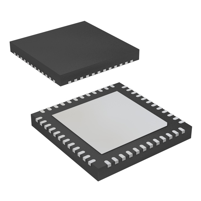
The CDCLVP1216RGZT from Texas Instruments is a high-performance 2:16 fanout buffer and multiplexer designed for precision clock distribution in demanding applications. Operating within a 2.375V to 3.6V supply range, this ROHS3-compliant, surface-mount IC supports input signals including LVCMOS, LVDS, LVPECL, and LVTTL, while delivering LVPECL outputs with exceptional signal integrity. With a maximum frequency of 2 GHz, it ensures low-jitter clock distribution, making it ideal for high-speed communication and data acquisition systems. Packaged in a 48-VQFN (RGZT) and rated for MSL 3 (168 hours), it combines reliability with compact form-factor suitability for space-constrained designs.
CDCLVP1216RGZT Features
- Flexible Input Compatibility: Accepts LVCMOS, LVDS, LVPECL, and LVTTL inputs, enabling seamless integration with diverse clock sources.
- High-Speed Performance: 2 GHz max frequency with ultra-low additive jitter, critical for 5G, optical networking, and high-speed SerDes applications.
- Differential I/O Support: Yes/Yes differential input/output capability ensures noise immunity and signal fidelity in noisy environments.
- Low Power Operation: Optimized for 2.375V–3.6V supply, balancing performance and power efficiency.
- Industrial Robustness: REACH unaffected and EAR99 classified, suitable for global export and harsh environments.
CDCLVP1216RGZT Applications
- Telecommunications: Clock distribution in base stations, routers, and optical transceivers requiring low-jitter, multi-output synchronization.
- Data Centers: Fanout for high-speed SerDes (PCIe, Ethernet) and memory interfaces.
- Test & Measurement: Precision timing in oscilloscopes, ATE systems, and radar equipment.
- Aerospace/Defense: Reliable clocking in avionics and radar systems due to its robust differential signaling.
Conclusion of CDCLVP1216RGZT
The CDCLVP1216RGZT stands out for its versatile input support, high-frequency operation, and industrial-grade reliability, making it a top choice for engineers designing high-speed, low-jitter clock networks. Its 2:16 fanout ratio and LVPECL output ensure consistent performance in telecom, data center, and mission-critical systems, while its compact 48-VQFN package addresses space and power constraints. For applications demanding precision, scalability, and noise immunity, this buffer/mux from Texas Instruments delivers unmatched value.
Tech Specifications
CDCLVP1216RGZT Documents
Download datasheets and manufacturer documentation for CDCLVP1216RGZT
CDCLVP1216 Conversion to 7" Reel 24/Jan/2014 CDCLVP1216 Copper Wire Base Metal 19/Jun/2014 Copper Wire Revision B 16/Dec/2014 Related Parts


Shopping Guide


.png?x-oss-process=image/format,webp/resize,h_32)


©2025 ERSA Electronics Corporation.