

Texas Instruments
CDCLVD110AVF
Clock Buffers, Drivers ICs

Not available to buy online? Want the lower wholesale price? Please Send RFQ to get best price, we will respond immediately


.png?x-oss-process=image/format,webp/resize,p_30)


CDCLVD110AVF Description
CDCLVD110AVF Description
The CDCLVD110AVF is a high-performance clock buffer and multiplexer designed by Texas Instruments, specifically tailored for applications requiring reliable and efficient clock signal distribution. This device features a 2:10 input-to-output ratio, making it ideal for fanout buffer and multiplexer applications. The CDCLVD110AVF supports differential signaling on both input and output, ensuring high signal integrity and minimal noise interference. It operates within a supply voltage range of 2.375V to 2.625V and can handle frequencies up to 1.1 GHz, making it suitable for high-speed clock distribution systems.
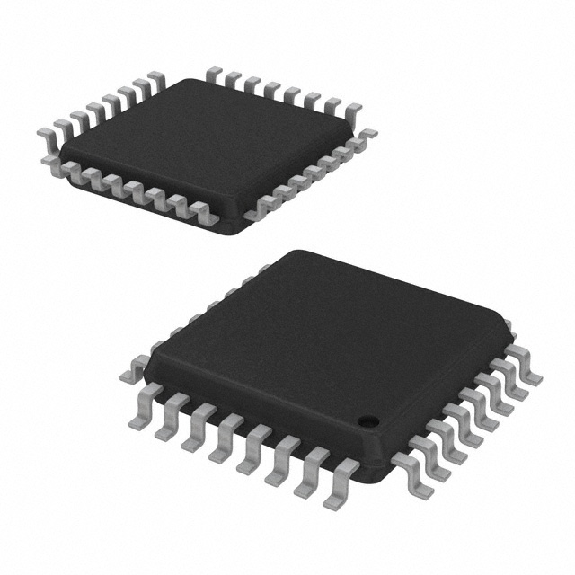
The CDCLVD110AVF is packaged in a 32LQFP format, which is ideal for surface mount applications, providing a compact and robust solution for modern electronic designs. The device is REACH unaffected and RoHS3 compliant, ensuring it meets the highest environmental and safety standards. With a moisture sensitivity level (MSL) of 1 (unlimited), the CDCLVD110AVF is suitable for a wide range of manufacturing processes without the risk of moisture-related damage.
CDCLVD110AVF Features
- High-Speed Performance: The CDCLVD110AVF supports a maximum frequency of 1.1 GHz, making it suitable for high-speed clock distribution in demanding applications.
- Differential Signaling: Both input and output support LVDS (Low Voltage Differential Signaling), ensuring high signal integrity and minimal noise interference.
- Flexible Input-to-Output Ratio: The 2:10 input-to-output ratio allows for efficient clock signal distribution, making it ideal for fanout buffer and multiplexer applications.
- Wide Supply Voltage Range: Operates within a supply voltage range of 2.375V to 2.625V, providing flexibility in power supply design.
- Surface Mount Compatibility: Packaged in a 32LQFP format, the CDCLVD110AVF is designed for surface mount applications, ensuring a compact and robust solution.
- Environmental Compliance: REACH unaffected and RoHS3 compliant, ensuring it meets the highest environmental and safety standards.
- Moisture Sensitivity Level: MSL 1 (unlimited), making it suitable for a wide range of manufacturing processes without the risk of moisture-related damage.
CDCLVD110AVF Applications
The CDCLVD110AVF is ideal for a variety of applications where high-speed clock distribution and signal integrity are critical. Some specific use cases include:
- Telecommunications: High-speed clock distribution in telecom equipment, ensuring reliable and efficient signal transmission.
- Data Centers: Fanout buffer applications in data center infrastructure, providing robust clock signal distribution for high-performance computing.
- Industrial Automation: Multiplexer applications in industrial automation systems, ensuring precise timing and control.
- Consumer Electronics: High-speed clock distribution in consumer electronics, such as high-definition displays and multimedia devices.
Conclusion of CDCLVD110AVF
The CDCLVD110AVF from Texas Instruments is a versatile and high-performance clock buffer and multiplexer, designed to meet the demands of modern electronic systems. Its high-speed performance, differential signaling, and wide supply voltage range make it an ideal choice for a variety of applications. The device's environmental compliance and robust packaging ensure it meets the highest standards for safety and reliability. Whether used in telecommunications, data centers, industrial automation, or consumer electronics, the CDCLVD110AVF provides a reliable and efficient solution for high-speed clock distribution and signal integrity.
Tech Specifications
CDCLVD110AVF Documents
Download datasheets and manufacturer documentation for CDCLVD110AVF
Mechanical Outline Drawing TI - PCN - 8-5-10 (PDF) Product Change Notification (PDF) CDCLVD110AVF Symbol & Footprint by SnapMagic Related Parts


Shopping Guide


.png?x-oss-process=image/format,webp/resize,h_32)


©2025 ERSA Electronics Corporation.