
Texas Instruments
CGS74LCT2524M
Clock Buffers, Drivers ICs


.png?x-oss-process=image/format,webp/resize,p_30)


CGS74LCT2524M Description
CGS74LCT2524M Description
The CGS74LCT2524M is a high-performance clock buffer IC designed by Texas Instruments, belonging to the 74LCT series. This device is specifically engineered to provide a 1:4 fanout distribution, making it ideal for applications requiring signal replication and distribution. The CGS74LCT2524M operates within a supply voltage range of 3V to 3.6V and can handle a maximum frequency of 75 MHz, ensuring reliable performance in high-speed clock distribution systems.
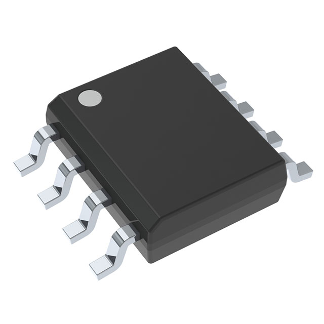
This IC features a CMOS input and TTL output, providing compatibility with a wide range of digital systems. The device is housed in an 8SOIC package, which is suitable for surface mount applications, making it ideal for compact and high-density PCB designs. The operating temperature range of 0°C to 70°C ensures that the CGS74L2CT524M can perform reliably in various environmental conditions.
CGS74LCT2524M Features
- High-Speed Performance: With a maximum operating frequency of 75 MHz, the CGS74LCT2524M ensures precise and efficient clock signal distribution.
- CMOS Input and TTL Output: This combination provides excellent compatibility with a wide range of digital systems, making it versatile for various applications.
- 1:4 Fanout Distribution: The device is designed to distribute a single input signal to four output signals, making it ideal for clock distribution in complex digital systems.
- Surface Mount Packaging: The 8SOIC package is suitable for surface mount applications, allowing for compact and high-density PCB designs.
- Wide Operating Voltage Range: The CGS74LCT2524M operates within a supply voltage range of 3V to 3.6V, providing flexibility in power supply requirements.
- Extended Temperature Range: The operating temperature range of 0°C to 70°C ensures reliable performance in various environmental conditions.
- Obsolete Status: While the product is marked as obsolete, it remains a reliable choice for legacy systems and applications where its specific features are required.
CGS74LCT2524M Applications
The CGS74LCT2524M is well-suited for a variety of applications where high-speed clock distribution is essential. Some specific use cases include:
- Digital Clock Distribution: Ideal for distributing clock signals in digital systems, ensuring precise timing and synchronization.
- High-Speed Communication Systems: Suitable for applications requiring high-speed data transmission and signal replication.
- Computer Systems: Useful in computer systems where clock signal distribution is critical for system performance.
- Telecommunications: Applicable in telecommunications equipment where reliable clock signal distribution is necessary for efficient operation.
- Industrial Control Systems: Provides robust performance in industrial environments where high-speed signal distribution is required.
Conclusion of CGS74LCT2524M
The CGS74LCT2524M from Texas Instruments is a high-performance clock buffer IC that offers significant advantages in high-speed clock distribution applications. Its 1:4 fanout distribution capability, combined with CMOS input and TTL output, ensures compatibility with a wide range of digital systems. The device's wide operating voltage range and extended temperature range make it versatile and reliable for various applications.
While the CGS74LCT2524M is marked as obsolete, it remains a valuable component for legacy systems and applications where its specific features are required. Its surface mount packaging and compact design make it suitable for high-density PCB designs, further enhancing its utility in modern electronics. Overall, the CGS74LCT2524M is a reliable choice for applications requiring efficient and precise clock signal distribution.
Tech Specifications
CGS74LCT2524M Documents
Download datasheets and manufacturer documentation for CGS74LCT2524M
 CGS74LCT2524
  CGS74LCT2524
 Shopping Guide


.png?x-oss-process=image/format,webp/resize,h_32)


