

Texas Instruments
CDCLVD1213RGTT
Clock Buffers, Drivers ICs

Not available to buy online? Want the lower wholesale price? Please Send RFQ to get best price, we will respond immediately


.png?x-oss-process=image/format,webp/resize,p_30)


CDCLVD1213RGTT Description
CDCLVD1213RGTT Description
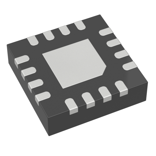
The CDCLVD1213RGTT from Texas Instruments is a high-performance 1:4 fanout buffer and divider designed for precision clock distribution in demanding electronic systems. This surface-mount IC supports CML, LVDS, and LVPECL input signals and delivers LVDS outputs, ensuring robust signal integrity with low jitter. Operating within a 2.375V to 2.625V supply range, it achieves a maximum frequency of 800 MHz, making it ideal for high-speed applications. Packaged in a 16-VQFN tape-and-reel (TR) format, it complies with ROHS3 and REACH environmental standards, with a Moisture Sensitivity Level (MSL) of 2 (1 year).
CDCLVD1213RGTT Features
- Wide Input Compatibility: Accepts CML, LVDS, and LVPECL inputs, offering flexibility in system design.
- Low Jitter Performance: Ensures minimal phase noise for high-frequency clock distribution.
- 1:4 Differential Output: Provides LVDS outputs with excellent signal integrity for synchronized multi-channel systems.
- Compact and Reliable: 16-VQFN package optimizes board space while maintaining thermal efficiency.
- Extended Temperature Range: Suitable for industrial and automotive applications requiring stable operation under varying conditions.
- Compliance: Meets ROHS3, REACH, and ECCN EAR99 standards, ensuring global usability.
CDCLVD1213RGTT Applications
This IC is particularly suited for:
- High-Speed Networking: Clock distribution in FPGA/ASIC-based systems, routers, and switches.
- Test & Measurement Equipment: Precision timing for oscilloscopes and signal analyzers.
- Wireless Infrastructure: Synchronization in 5G base stations and RF transceivers.
- Data Centers: Low-latency clocking for servers and storage systems.
- Automotive Electronics: ADAS and infotainment systems requiring robust signal integrity.
Conclusion of CDCLVD1213RGTT
The CDCLVD1213RGTT stands out as a versatile, high-performance clock buffer, combining wide input compatibility, low jitter, and compact packaging. Its ability to handle 800 MHz signals with precision makes it indispensable in high-speed digital systems, while compliance with environmental standards ensures reliability in industrial applications. Engineers can leverage its differential signaling and flexible input options to enhance system synchronization in networking, automotive, and test equipment designs.
Tech Specifications
CDCLVD1213RGTT Documents
Download datasheets and manufacturer documentation for CDCLVD1213RGTT
Wafer Fab Site 02/Dec/2022 CDCLVD1213 QFN,VSSOP Reel Size 12/Sep/2013 Mult Dev Material Chg 29/Mar/2018 Related Parts


Shopping Guide


.png?x-oss-process=image/format,webp/resize,h_32)


©2025 ERSA Electronics Corporation.