

Texas Instruments
CDCLVD1212RHAT
Clock Buffers, Drivers ICs

Not available to buy online? Want the lower wholesale price? Please Send RFQ to get best price, we will respond immediately


.png?x-oss-process=image/format,webp/resize,p_30)


CDCLVD1212RHAT Description
CDCLVD1212RHAT Description
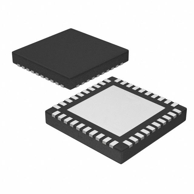
The CDCLVD1212RHAT from Texas Instruments is a high-performance 1:6 differential clock fanout buffer and multiplexer designed for precision timing applications. Housed in a compact 40-VQFN package, this surface-mount device supports LVCMOS, LVDS, and LVPECL input signals and delivers 12 LVDS outputs with a 2:12 input-to-output ratio. Operating within a 2.375V to 2.625V supply range, it achieves a maximum frequency of 800 MHz, making it ideal for high-speed data transmission and synchronization systems. The device is RoHS3 compliant, REACH unaffected, and rated for MSL 3 (168 hours), ensuring reliability in industrial and commercial environments.
CDCLVD1212RHAT Features
- Wide Input Compatibility: Accepts LVCMOS, LVDS, and LVPECL inputs for flexible system integration.
- Low-Jitter Performance: Ensures minimal signal distortion, critical for high-speed communication and clock distribution.
- High Fanout Capability: Distributes 12 LVDS outputs from 1 or 2 inputs, reducing the need for additional buffers.
- 800 MHz Maximum Frequency: Supports demanding applications such as FPGA/ASIC clocking, networking, and telecom infrastructure.
- Robust Power Supply Range (2.375V–2.625V): Optimized for low-power operation without compromising signal integrity.
- Industrial-Grade Reliability: RoHS3 compliant, REACH unaffected, and MSL 3-rated for extended operational life.
CDCLVD1212RHAT Applications
- Telecommunications: Clock distribution in 5G base stations, optical transceivers, and network switches.
- Data Centers: Synchronization for high-speed servers, storage systems, and FPGA-based accelerators.
- Test & Measurement Equipment: Precision timing for oscilloscopes, signal generators, and automated test systems.
- Aerospace & Defense: Reliable clocking in radar systems, avionics, and secure communication devices.
- Consumer Electronics: Low-jitter clocking for high-resolution displays and multimedia interfaces.
Conclusion of CDCLVD1212RHAT
The CDCLVD1212RHAT stands out as a versatile, high-performance clock buffer, offering low jitter, wide input compatibility, and scalable fanout in a compact form factor. Its 800 MHz capability and robust design make it a preferred choice for high-speed digital systems where timing accuracy is critical. Whether deployed in telecom infrastructure, data centers, or industrial electronics, this device ensures reliable signal distribution with minimal added noise, enhancing system performance while reducing component count.
Tech Specifications
CDCLVD1212RHAT Documents
Download datasheets and manufacturer documentation for CDCLVD1212RHAT
Wafer Fab Site 02/Dec/2022 CDCLVD1212 Datasheet Conversion to 7" Reel 24/Jan/2014 CDCLVD1212 Datasheet Mult Dev Material Chg 29/Mar/2018 Related Parts


Shopping Guide


.png?x-oss-process=image/format,webp/resize,h_32)


©2025 ERSA Electronics Corporation.