

Texas Instruments
CDCLVP111MVFREP
Clock Buffers, Drivers ICs

Not available to buy online? Want the lower wholesale price? Please Send RFQ to get best price, we will respond immediately


.png?x-oss-process=image/format,webp/resize,p_30)


CDCLVP111MVFREP Description
CDCLVP111MVFREP Description
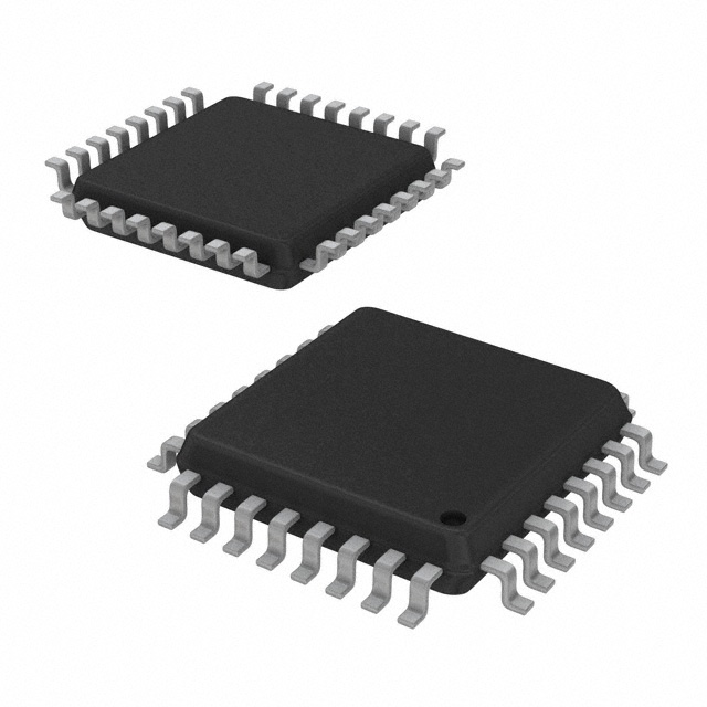
The CDCLVP111MVFREP from Texas Instruments is a high-performance 1:10 differential fanout buffer and multiplexer designed for precision clock distribution in demanding applications. This surface-mount IC supports a wide input voltage range of 2.375V to 3.8V and delivers LVPECL outputs, ensuring robust signal integrity for high-speed systems. With a maximum frequency of 3.5 GHz, it is engineered for low-jitter operation, making it ideal for telecommunications, networking, and high-speed data acquisition systems. The device accepts multiple input standards (CML, LVDS, LVPECL, SSTL), offering exceptional flexibility in system design. Packaged in a 32-LQFP tape-and-reel (TR) format, it complies with ROHS3 and REACH environmental standards.
CDCLVP111MVFREP Features
- High-Speed Performance: Supports frequencies up to 3.5 GHz with minimal jitter, critical for synchronous systems.
- Versatile Input Compatibility: Accepts CML, LVDS, LVPECL, and SSTL inputs, enabling seamless integration with diverse logic families.
- Low-Power Operation: Optimized for 2.375V–3.8V supply, balancing performance and energy efficiency.
- Differential Signaling: Yes/Yes differential input/output architecture ensures noise immunity and signal fidelity.
- Compact & Reliable: 32-LQFP package with MSL 3 (168 hours) moisture sensitivity, suitable for automated assembly.
- Industry Compliance: ROHS3, REACH Unaffected, and EAR99 classifications simplify global deployment.
CDCLVP111MVFREP Applications
- Telecom Infrastructure: Clock distribution in 5G base stations, optical transceivers, and network switches.
- Data Centers: Synchronization of high-speed FPGAs, ASICs, and SerDes interfaces.
- Test & Measurement: Precision timing for oscilloscopes, ATE systems, and radar equipment.
- Aerospace & Defense: Resilient clocking in avionics and secure communications due to robust differential signaling.
Conclusion of CDCLVP111MVFREP
The CDCLVP111MVFREP stands out as a high-speed, low-jitter solution for critical clock distribution challenges. Its multi-standard input support, differential robustness, and compact form factor make it superior to generic buffers in high-reliability applications. Whether in telecom, data centers, or aerospace, this device ensures timing accuracy and system stability, backed by Texas Instruments’ proven quality and compliance.
Tech Specifications
CDCLVP111MVFREP Documents
Download datasheets and manufacturer documentation for CDCLVP111MVFREP
CDCLVP111-EP CDCLVP111-EP Related Parts


Shopping Guide


.png?x-oss-process=image/format,webp/resize,h_32)


©2025 ERSA Electronics Corporation.