
Texas Instruments
CDC3S04YFFR
Clock Buffers, Drivers ICs


.png?x-oss-process=image/format,webp/resize,p_30)


CDC3S04YFFR Description
CDC3S04YFFR Description
The CDC3S04YFFR is a high-performance, 1:4 fanout buffer clock distribution IC designed by Texas Instruments. This device is specifically engineered to provide reliable and efficient clock signal distribution in various electronic systems. With a maximum operating frequency of 52 MHz, the CDC3S04YFFR ensures precise timing and synchronization across multiple circuits. It operates within a supply voltage range of 1.65V to 1.95V, making it suitable for low-power applications.
CDC3S04YFFR Features
- High Fanout Capability: The 1:4 ratio input to output fanout capability allows the CDC3S04YFFR to distribute a single clock signal to four output channels efficiently. This feature is particularly beneficial in systems requiring multiple clock signals derived from a single source.
- Surface Mount Technology: The surface mount mounting type ensures ease of integration into compact and high-density PCB designs. This is advantageous for modern electronics where space is a critical consideration.
- Low Power Consumption: Operating within a voltage range of 1.65V to 1.95V, the CDC3S04YFFR is designed for low power consumption, making it ideal for battery-operated and energy-efficient applications.
- Compliance and Reliability: The CDC3S04YFFR is REACH unaffected and ROHS3 compliant, ensuring it meets stringent environmental and safety standards. This compliance is crucial for manufacturers aiming to adhere to global regulations.
- Moisture Sensitivity Level With: a moisture sensitivity level (MSL) of 1 (unlimited), the CDC3S04YFFR is highly resistant to moisture, enhancing its reliability and longevity in various environmental conditions.
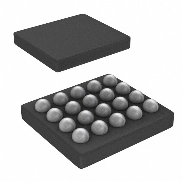
- Packaging: The device is packaged in a 20-DSBGA format, which is part of the Tape & Reel (TR) packaging type. This packaging ensures ease of handling and integration into automated assembly processes.
CDC3S04YFFR Applications
The CDC3S04YFFR is ideal for a wide range of applications where precise clock signal distribution is required. Some specific use cases include:
- Telecommunications: In communication systems, the CDC3S04YFFR can be used to distribute clock signals across multiple components, ensuring synchronized operation and minimizing jitter.
- Data Centers: For server and storage systems, the CDC3S04YFFR provides reliable clock distribution, enhancing the performance and reliability of high-speed data processing.
- Consumer Electronics: In devices such as smartphones, tablets, and smart TVs, the CDC3S04YFFR can distribute clock signals to various subsystems, ensuring synchronized operation and improving overall performance.
- Industrial Automation: In industrial control systems, the CDC3S04YFFR can distribute clock signals to multiple sensors and actuators, ensuring precise timing and control.
Conclusion of CDC3S04YFFR
The CDC3S04YFFR from Texas Instruments is a robust and versatile clock distribution IC that offers significant advantages over similar models. Its high fanout capability, low power consumption, and compliance with environmental standards make it an ideal choice for a wide range of applications. The device's surface mount technology and compact packaging further enhance its suitability for modern, space-constrained designs. Whether used in telecommunications, data centers, consumer electronics, or industrial automation, the CDC3S04YFFR ensures reliable and efficient clock signal distribution, making it a valuable component in any electronic system.
Tech Specifications
CDC3S04YFFR Documents
Download datasheets and manufacturer documentation for CDC3S04YFFR
 Mechanical Outline Drawing Function Diagram
  Power Supply Rejection to Noise in Sinusoidal Clock Buffers: CDC3S04 (Rev. A) Using the CDC3S04
 Shopping Guide


.png?x-oss-process=image/format,webp/resize,h_32)


