
 German
 Japanese
 Portuguese
 Korea
Korea
 Mexico
 Dutch
Dutch


Texas Instruments
CDCS503PW

Why Choose Us?
Professional Platform
B2B & B2C purchasingDelivery at full speed
1-2 days deliveryWide variety
Original manufacturers365 days guarantee
Responsible quality
.png)


Tech Specifications
CDCS503PW Description
CDCS503PW Description
The CDCS503PW is a high-performance clock buffer IC designed by Texas Instruments, ideal for applications requiring a reliable and efficient clock signal distribution. This device features a 1:1 input-to-output ratio, ensuring that the input clock signal is accurately replicated at the output without any differential signaling, which is suitable for many digital systems. The CDCS503PW is designed to operate with LVCMOS input and output levels, making it compatible with a wide range of digital circuits. It supports a supply voltage range of 3V to 3.6V, providing flexibility in power supply design.
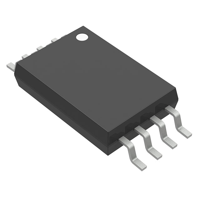
The CDCS503PW is housed in an 8-pin TSSOP package, which is suitable for surface-mount applications, ensuring ease of integration into modern PCB designs. With a maximum operating frequency of 108 MHz, this IC is well-suited for high-speed clock distribution in various electronic systems. The device is REACH unaffected and RoHS3 compliant, adhering to stringent environmental and safety standards.
CDCS503PW Features
- 1:1 Input-to-Output Ratio: Ensures accurate replication of the input clock signal, maintaining signal integrity.
- LVCMOS Compatibility: Supports LVCMOS input and output levels, making it compatible with a wide range of digital circuits.
- Wide Supply Voltage Range: Operates within a 3V to 3.6V range, offering flexibility in power supply design.
- High-Speed Performance: Capable of operating up to 108 MHz, suitable for high-speed clock distribution.
- Surface-Mount Packaging: The 8-pin TSSOP package is ideal for surface-mount applications, ensuring ease of integration.
- Environmental Compliance: REACH unaffected and RoHS3 compliant, ensuring adherence to environmental and safety standards.
- Moisture Sensitivity Level 1: Suitable for unlimited storage conditions, reducing handling and storage concerns.
CDCS503PW Applications
The CDCS503PW is ideal for a variety of applications where reliable clock signal distribution is crucial. Some specific use cases include:
- Telecommunications: Used in base stations and network equipment for clock distribution.
- Computing: Ideal for server and workstation motherboards to ensure accurate clock signal distribution.
- Consumer Electronics: Suitable for high-speed devices such as gaming consoles and smart TVs.
- Industrial Systems: Used in automation and control systems where precise timing is essential.
- Medical Equipment: Ensures accurate timing in medical imaging and diagnostic devices.
Conclusion of CDCS503PW
The CDCS503PW from Texas Instruments is a robust and versatile clock buffer IC that offers high-speed performance and compatibility with LVCMOS levels. Its 1:1 input-to-output ratio and surface-mount packaging make it an excellent choice for a wide range of applications, from telecommunications to consumer electronics. The device's environmental compliance and moisture sensitivity level 1 rating further enhance its reliability and ease of use. Whether you are designing a high-speed computing system or a precision medical device, the CDCS503PW provides the performance and reliability needed to ensure accurate clock signal distribution.
FAQ
| Quantity | Unit Price | Ext. Price |
|---|---|---|
| 1+ | $1.59280 | $1.59 |
| 10+ | $1.16776 | $11.68 |
| 25+ | $1.06269 | $26.57 |
| 150+ | $0.92042 | $138.06 |
| 300+ | $0.88200 | $264.60 |
Not available to buy online? Want the lower wholesale price? Please Send RFQ to get best price, we will respond immediately


.png?x-oss-process=image/format,webp/resize,h_32)


