
Texas Instruments
CDCVF2505IDRQ1
Clock Generators & Support Products


.png?x-oss-process=image/format,webp/resize,p_30)


CDCVF2505IDRQ1 Description
CDCVF2505IDRQ1 Description
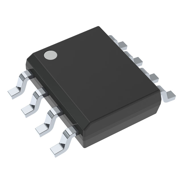
The CDCVF2505IDRQ1 is an IC PLL Clock Driver designed by Texas Instruments, specifically tailored for automotive applications. This device is housed in an 8SOIC package and offers a robust solution for clock distribution and synchronization. With a maximum operating frequency of 200MHz, it provides reliable performance in demanding environments.
CDCVF2505IDRQ1 Features
- PLL with Bypass Capability: The CDCVF2505IDRQ1 incorporates a Phase-Locked Loop (PLL) that can be bypassed, offering flexibility in clock management. This feature allows designers to optimize performance based on specific application requirements.
- LVTTL Input and Output: The device supports LVTTL input and output levels, ensuring compatibility with a wide range of digital systems. This compatibility simplifies integration into existing designs.
- 3V to 3.6V Supply Voltage: The wide supply voltage range of 3V to 3.6V ensures stable operation across various power supply conditions, enhancing the device's versatility.
- 1:5 Input to Output Ratio: The CDCVF2505IDRQQ1 features a 1:5 input to output ratio, effectively multiplying the input clock signal to drive multiple outputs. This capability is crucial for applications requiring multiple synchronized clock signals.
- Surface Mount Packaging: The surface mount package type facilitates easy integration into compact and high-density PCB designs, making it suitable for space-constrained automotive applications.
- Automotive Grade: Certified for automotive use, the CDCVF2505IDRQ1 meets stringent reliability and performance standards required for automotive electronics.
- Compliance and Reliability: The device is REACH unaffected and ROHS3 compliant, ensuring it meets environmental and safety regulations. Additionally, with a Moisture Sensitivity Level (MSL) of 1, it is suitable for unlimited storage and handling.
- Tape & Reel Packaging: The CDCVF2505IDRQ1 is available in tape & reel packaging, which is ideal for automated assembly processes and ensures consistent quality during manufacturing.
CDCVF2505IDRQ1 Applications
The CDCVF2505IDRQ1 is particularly well-suited for automotive applications where reliable clock distribution and synchronization are critical. Specific use cases include:
- Automotive Infotainment Systems: Providing stable clock signals for processors and peripherals in infotainment systems.
- Advanced Driver Assistance Systems (ADAS): Ensuring precise timing for sensors and control units in ADAS applications.
- ECU (Electronic Control Unit) Applications: Supplying synchronized clock signals for various ECUs in the vehicle.
- High-Speed Communication Interfaces: Distributing clock signals for high-speed interfaces such as CAN, LIN, and Ethernet.
Conclusion of CDCVF2505IDRQ1
The CDCVF2505IDRQ1 from Texas Instruments stands out as a reliable and versatile PLL clock driver for automotive applications. Its unique features, such as the PLL with bypass capability, wide supply voltage range, and LVTTL compatibility, provide significant advantages over similar models. The device's automotive-grade certification and compliance with environmental regulations make it an ideal choice for demanding automotive environments. Whether used in infotainment systems, ADAS, or high-speed communication interfaces, the CDCVF2505IDRQ1 ensures precise clock distribution and synchronization, enhancing the overall performance and reliability of automotive electronic systems.
Tech Specifications
CDCVF2505IDRQ1 Documents
Download datasheets and manufacturer documentation for CDCVF2505IDRQ1
 Mult Dev 30/Oct/2019
  CDCVF2505-Q1
  CDCVF2505-Q1
 Shopping Guide


.png?x-oss-process=image/format,webp/resize,h_32)


