
 German
 Japanese
 Portuguese
 Korea
Korea
 Mexico
 Dutch
Dutch


Texas Instruments
DS90LV110TMTCX

Why Choose Us?
Professional Platform
B2B & B2C purchasingDelivery at full speed
1-2 days deliveryWide variety
Original manufacturers365 days guarantee
Responsible quality
.png)


Tech Specifications
DS90LV110TMTCX Description
DS90LV110TMTCX Description
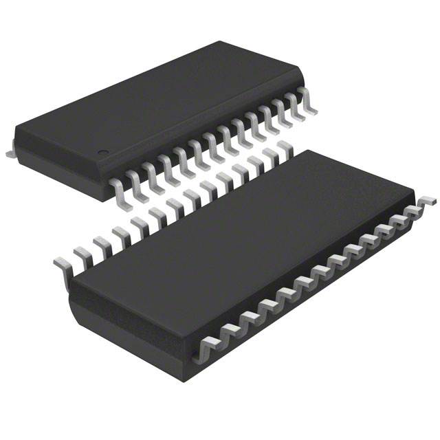
The DS90LV110TMTCX is a high-performance fanout buffer (distribution) IC designed for clock buffering applications, manufactured by Texas Instruments. This device features a 1:10 input-to-output ratio, making it ideal for distributing clock signals across multiple circuits. It supports differential signaling, with both input and output being differential, ensuring high signal integrity and reduced electromagnetic interference (EMI). The DS90LV110TMTCX operates on a supply voltage range of 3V to 3.6V and can handle frequencies up to 400 MHz, making it suitable for high-speed applications. The device is packaged in a 28-pin TSSOP surface-mount package, which is ideal for compact and space-constrained designs. Although this product is now obsolete, it remains a notable solution in the clock buffers and drivers ICs category.
DS90LV110TMTCX Features
- High-Speed Performance: With a maximum operating frequency of 400 MHz, the DS90LV110TMTCX ensures precise and reliable clock signal distribution at high speeds.
- Differential Signaling: The device supports differential signaling (LVDS, LVPECL, PECL) for both input and output, which enhances signal integrity and reduces EMI, making it suitable for high-speed and sensitive applications.
- Flexible Input and Output: The DS90LV110TMTCX can accept LVDS, LVPECL, and PECL input signals and provides LVDS output, offering flexibility in interfacing with various clock sources and loads.
- Surface-Mount Packaging: The 28-pin TSSOP package is designed for surface-mount technology, enabling compact and efficient PCB layouts.
- Supply Voltage Range: The device operates within a 3V to 3.6V supply voltage range, providing compatibility with a wide range of power supply systems.
- Moisture Sensitivity Level: With an MSL of 3 (168 hours), the DS90LV110TMTCX is suitable for manufacturing processes that require controlled environments to prevent moisture-related issues.
- REACH Compliance: The DS90LV110TMTCX is REACH unaffected, ensuring compliance with environmental and safety regulations.
DS90LV110TMTCX Applications
The DS90LV110TMTCX is ideal for applications that require high-speed clock distribution and signal integrity. Some specific use cases include:
- Telecommunications: In high-speed communication systems, the DS90LV110TMTCX can distribute clock signals across multiple components, ensuring synchronized operation.
- Networking Equipment: For networking devices such as routers and switches, the fanout buffer can provide reliable clock distribution to various modules.
- High-Speed Data Processing: In systems that require high-speed data processing, such as servers and workstations, the DS90LV110TMTCX can distribute clock signals to multiple processing units.
- Consumer Electronics: In devices such as high-definition televisions and gaming consoles, the DS90LV110TMTCX can distribute clock signals to various components, ensuring synchronized operation and high performance.
Conclusion of DS90LV110TMTCX
The DS90LV110TMTCX is a robust and versatile fanout buffer IC designed for high-speed clock distribution applications. Its support for differential signaling, wide supply voltage range, and high-frequency performance make it a reliable choice for various electronic systems. Although now obsolete, the DS90LV110TMTCX remains a notable solution in the clock buffers and drivers ICs category, offering unique features and advantages over similar models. For applications requiring high-speed clock distribution and signal integrity, the DS90LV110TMTCX is an ideal choice.
FAQ
Not available to buy online? Want the lower wholesale price? Please Send RFQ to get best price, we will respond immediately


.png?x-oss-process=image/format,webp/resize,h_32)


